
5SGSMD3H2F35C3N
| Part Description |
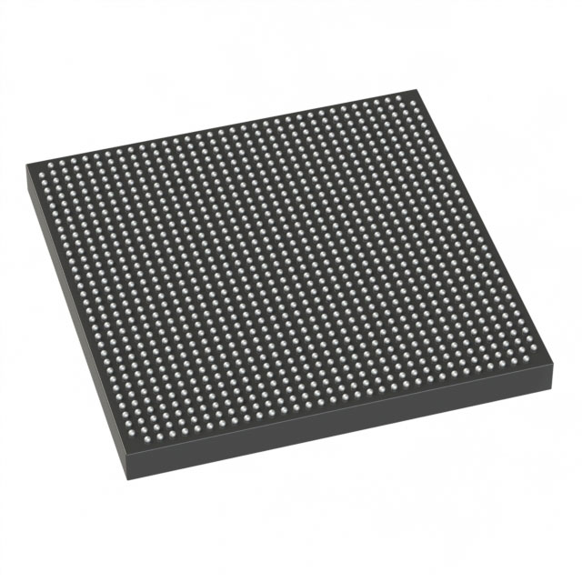
Stratix® V GS Field Programmable Gate Array (FPGA) IC 432 13312000 236000 1152-BBGA, FCBGA |
|---|---|
| Quantity | 306 Available (as of June 9, 2026) |

| Product Category | Field Programmable Gate Array (FPGA) |
|---|---|
| Manufacturer | Intel |
| Manufacturing Status | Obsolete |
| Manufacturer Standard Lead Time | Contact Us |
| Datasheet |
Specifications & Environmental
| Device Package | 1152-FBGA (35x35) | Grade | Commercial | Operating Temperature | 0°C – 85°C | ||
|---|---|---|---|---|---|---|---|
| Package / Case | 1152-BBGA, FCBGA | Number of I/O | 432 | Voltage | 820 mV - 880 mV | ||
| Mounting Method | Surface Mount | RoHS Compliance | RoHS Compliant | REACH Compliance | REACH Unknown | ||
| Moisture Sensitivity Level | 3 (168 Hours) | Number of LABs/CLBs | 89000 | Number of Logic Elements/Cells | 236000 | ||
| Number of Gates | N/A | ECCN | 3A001A2C | HTS Code | 8542.39.0001 | ||
| Qualification | N/A | Total RAM Bits | 13312000 |
Overview of 5SGSMD3H2F35C3N – Stratix V GS FPGA, 432 I/O, 236,000 logic elements
The 5SGSMD3H2F35C3N is a Stratix® V GS field-programmable gate array (FPGA) from Intel, built on a 28‑nm process and targeted at transceiver‑based, DSP‑centric applications. This commercial‑grade device combines high logic density, substantial on‑chip memory, and a large I/O count to address bandwidth‑heavy designs and complex signal processing tasks.
With 236,000 logic elements, approximately 13.3 Mbits of embedded memory, and 432 I/O, the device is suited for applications that require deep processing resources, extensive interfacing, and integrated high‑speed serial connectivity options offered within the Stratix V family.
Key Features
- Core and Process 28‑nm TSMC process technology used across the Stratix V family; device operates with a core supply range of 820 mV to 880 mV.
- Logic Capacity 236,000 logic elements to implement complex FPGA designs and large-scale custom logic.
- Embedded Memory Approximately 13.3 Mbits of on‑chip RAM provided by M20K memory blocks common to the Stratix V architecture.
- DSP Resources Stratix V GS family devices include variable‑precision DSP blocks (family capability includes support for up to 3,926 18×18 or 1,963 27×27 multipliers), enabling high‑performance arithmetic and signal processing implementations.
- High‑speed Transceivers GS devices in the Stratix V family offer integrated transceivers with 14.1‑Gbps data‑rate capability for backplane and optical interfaces.
- I/O and Packaging 432 I/O pins in a surface‑mount 1152‑BBGA (FCBGA) package / supplier package 1152‑FBGA (35×35) for dense board integration and routing.
- Clocking and System Integration Family architecture includes fractional PLLs, multi‑track routing, and a comprehensive fabric clocking network to support complex timing domains.
- Grade and Environmental Commercial‑grade device rated for 0 °C to 85 °C operating temperature and RoHS compliant.
Typical Applications
- High‑performance DSP systems Use the abundant variable‑precision DSP blocks and large logic capacity for signal processing pipelines, filters, and real‑time computation tasks.
- Optical and Backplane Interfaces Integrated 14.1‑Gbps transceivers make the device suitable for backplane and optical interface applications requiring high serial bandwidth.
- Network and Packet Processing Large on‑chip memory and extensive logic enable packet processing, traffic management, and other data‑intensive networking functions.
- Broadcast and Military Communications Architected to support transceiver‑based, DSP‑centric applications common in broadcast and military communications equipment.
Unique Advantages
- High logic density: 236,000 logic elements allow implementation of large, feature‑rich FPGA designs without immediate partitioning.
- Significant embedded memory: Approximately 13.3 Mbits of on‑chip RAM reduce external memory requirements and simplify board-level design.
- Integrated high‑speed connectivity: GS family transceivers providing up to 14.1 Gbps ease integration of high‑bandwidth interfaces.
- Comprehensive DSP support: Variable‑precision DSP blocks enable efficient implementation of complex arithmetic operations and signal processing algorithms.
- Dense I/O and package: 432 I/O in a 1152‑BBGA (35×35) FCBGA package supports compact, high‑pin‑count board designs.
- Commercial readiness: RoHS compliance and a 0 °C–85 °C operating range match standard commercial product deployment environments.
Why Choose 5SGSMD3H2F35C3N?
The 5SGSMD3H2F35C3N balances large logic capacity, plentiful embedded memory, and integrated high‑speed transceivers within the Stratix V GS family architecture. It is positioned for engineers building DSP‑intensive, bandwidth‑centric systems that require a combination of processing density, on‑chip RAM, and plentiful I/O in a compact surface‑mount package.
This device is well suited to teams developing data‑intensive networking, broadcast, and high‑performance computing applications who need scalable FPGA resources backed by the Stratix V feature set, including advanced clocking, DSP blocks, and integrated transceiver capability.
Request a quote or submit an inquiry to evaluate 5SGSMD3H2F35C3N for your next FPGA design.


Date Founded: 1968
Headquarters: Santa Clara, California, USA
Employees: 130,000+
Revenue: $54.23 Billion
Certifications and Memberships: ISO9001:2015, ISO14001:2015, ISO17025:2017, ISO27001:2022, ISO45001:2018, ISO50001:2018


