
5SGSMD3H2F35I2LN
| Part Description |
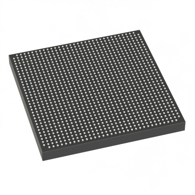
Stratix® V GS Field Programmable Gate Array (FPGA) IC 432 13312000 236000 1152-BBGA, FCBGA |
|---|---|
| Quantity | 470 Available (as of June 15, 2026) |

| Product Category | Field Programmable Gate Array (FPGA) |
|---|---|
| Manufacturer | Intel |
| Manufacturing Status | Obsolete |
| Manufacturer Standard Lead Time | Contact Us |
| Datasheet |
Specifications & Environmental
| Device Package | 1152-FBGA (35x35) | Grade | Industrial | Operating Temperature | -40°C – 100°C | ||
|---|---|---|---|---|---|---|---|
| Package / Case | 1152-BBGA, FCBGA | Number of I/O | 432 | Voltage | 820 mV - 880 mV | ||
| Mounting Method | Surface Mount | RoHS Compliance | RoHS Compliant | REACH Compliance | REACH Unknown | ||
| Moisture Sensitivity Level | 3 (168 Hours) | Number of LABs/CLBs | 89000 | Number of Logic Elements/Cells | 236000 | ||
| Number of Gates | N/A | ECCN | 3A001A2C | HTS Code | 8542.39.0001 | ||
| Qualification | N/A | Total RAM Bits | 13312000 |
Overview of 5SGSMD3H2F35I2LN – Stratix® V GS FPGA, 236,000 logic elements, 432 I/O, 1152-BBGA
The 5SGSMD3H2F35I2LN is an Intel Stratix V GS field-programmable gate array (FPGA) built on the Stratix V family architecture. It combines a high logic density of 236,000 logic elements with abundant embedded memory and DSP resources for transceiver-based, DSP-centric applications.
Targeted at data- and signal-processing markets, this industrial-grade device supports high-throughput DSP implementations and transceiver interfaces while providing a compact surface-mount FCBGA package and an extended operating temperature range for deployment in demanding environments.
Key Features
- Core architecture — Stratix V family device built on 28‑nm process technology with a redesigned adaptive logic module (ALM) and a multi-track routing fabric.
- Logic capacity — 236,000 logic elements suitable for complex FPGA designs and large-scale logic implementations.
- Embedded memory — Approximately 13.3 Mbits of on-chip RAM (13,312,000 bits) for buffering, packet processing, and intermediate data storage.
- DSP resources — GS variant supports an abundance of variable-precision DSP blocks, including support for up to 3,926 18×18 or 1,963 27×27 multipliers for high-performance signal processing.
- Transceiver capability — GS devices in the Stratix V family provide integrated transceivers with 14.1‑Gbps data-rate capability for backplane and optical interface applications.
- I/O and package — 432 user I/O pins in a 1152‑BBGA (FCBGA) supplier package format (1152‑FBGA, 35×35 mm) for dense board-level integration; surface-mount mounting type.
- Power — Core supply operating range 820 mV to 880 mV to match system power-rail planning.
- Thermal and grade — Industrial grade with an operating temperature range of −40°C to 100°C for use across extended-temperature environments.
- Compliance — RoHS‑compliant device suitable for environmentally regulated designs.
Typical Applications
- High-performance DSP systems — Use the device’s large DSP block count and embedded memory for signal filtering, FFTs, and other compute-intensive algorithms.
- Optical and backplane interfaces — Integrated transceivers with 14.1‑Gbps capability enable high-speed backplane and optical link implementations.
- Network and packet processing — Combine abundant logic elements and on-chip RAM for packet buffering, classification, and protocol handling in networking equipment.
- Military and broadcast systems — Industrial-grade temperature range and FCBGA packaging support deployment in demanding communications and broadcast applications.
Unique Advantages
- Large programmable fabric: 236,000 logic elements provide the capacity to implement complex custom logic, accelerators, and control functions without external ASICs.
- Significant on-chip memory: Approximately 13.3 Mbits of embedded RAM reduces external memory dependence and improves data-path latency.
- Strong DSP throughput: High counts of 18×18 and 27×27 multipliers accelerate fixed- and variable-precision signal processing workloads.
- High-speed I/O integration: 432 I/O and integrated transceivers simplify board-level design for high-bandwidth interfaces.
- Industrial temperature qualification: −40°C to 100°C operating range enables use in extended-temperature and ruggedized systems.
- Compact, manufacturable package: 1152‑BBGA (35×35 mm) FCBGA surface-mount package supports high-density PCB integration and automated assembly.
Why Choose 5SGSMD3H2F35I2LN?
The 5SGSMD3H2F35I2LN positions itself as a high-capacity, DSP-oriented Stratix V GS FPGA combining sizable logic resources, substantial embedded memory, and dedicated DSP multipliers with integrated transceiver capability. Its industrial-grade temperature range and compact FCBGA package make it suitable for demanding, bandwidth- and compute-centric designs that require on-chip memory and signal-processing acceleration.
Design teams targeting data-intensive communications, high-performance computing, or broadcast and military signal-processing systems can leverage this device’s balance of logic, memory, DSP, and I/O to reduce external components, streamline board design, and scale performance within the Stratix V family architecture.
Request a quote or submit a request for pricing and availability to evaluate 5SGSMD3H2F35I2LN for your next design.


Date Founded: 1968
Headquarters: Santa Clara, California, USA
Employees: 130,000+
Revenue: $54.23 Billion
Certifications and Memberships: ISO9001:2015, ISO14001:2015, ISO17025:2017, ISO27001:2022, ISO45001:2018, ISO50001:2018


