
5SGSMD4E2H29C1N
| Part Description |
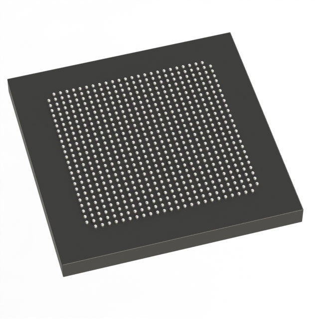
Stratix® V GS Field Programmable Gate Array (FPGA) IC 360 19456000 360000 780-BBGA, FCBGA |
|---|---|
| Quantity | 930 Available (as of June 15, 2026) |

| Product Category | Field Programmable Gate Array (FPGA) |
|---|---|
| Manufacturer | Intel |
| Manufacturing Status | Obsolete |
| Manufacturer Standard Lead Time | Contact Us |
| Datasheet |
Specifications & Environmental
| Device Package | 780-HBGA (33x33) | Grade | Commercial | Operating Temperature | 0°C – 85°C | ||
|---|---|---|---|---|---|---|---|
| Package / Case | 780-BBGA, FCBGA | Number of I/O | 360 | Voltage | 870 mV - 930 mV | ||
| Mounting Method | Surface Mount | RoHS Compliance | RoHS Compliant | REACH Compliance | REACH Unknown | ||
| Moisture Sensitivity Level | 3 (168 Hours) | Number of LABs/CLBs | 135840 | Number of Logic Elements/Cells | 360000 | ||
| Number of Gates | N/A | ECCN | 3A001A2C | HTS Code | 8542.39.0001 | ||
| Qualification | N/A | Total RAM Bits | 19456000 |
Overview of 5SGSMD4E2H29C1N – Stratix® V GS FPGA, 360 I/Os, 360,000 logic elements, 780-BBGA (FCBGA)
The 5SGSMD4E2H29C1N is an Intel Stratix V GS field-programmable gate array (FPGA) in a 780-ball FCBGA package. It implements the Stratix V architecture on a 28‑nm process and targets transceiver‑based, DSP‑centric designs.
With 360,000 logic elements, approximately 19.456 Mbits of embedded memory, and 360 I/Os, this device is suited for high‑performance applications that require large logic capacity, significant on‑chip RAM, and extensive I/O connectivity.
Key Features
- Core Architecture Stratix V family architecture implemented in a 28‑nm process with an enhanced core and adaptive logic modules for high-performance logic synthesis.
- Logic Capacity 360,000 logic elements to support large, complex designs and extensive logic integration on a single device.
- Embedded Memory Approximately 19.456 Mbits of on‑chip RAM to support buffering, packet processing, and intermediate data storage.
- DSP Resources GS‑variant device family includes abundant variable‑precision DSP blocks; Stratix V GS devices support up to 3,926 18×18 or 1,963 27×27 multipliers for compute‑intensive signal processing tasks.
- Transceiver and Protocol Support Stratix V family integrates high‑speed transceivers (GS devices support 14.1‑Gbps data‑rate capability) and an Embedded HardCopy Block for hardened PCIe Gen3/Gen2/Gen1 IP instantiation.
- I/O and Packaging 360 configurable I/Os and a 780‑ball FCBGA (33×33) package, enabling high pin‑count board designs and dense system integration.
- Power and Voltage Core supply range specified at 0.870 V to 0.930 V, allowing designers to plan power delivery and thermal budgets precisely.
- Operating Conditions Commercial grade with an operating temperature range of 0 °C to 85 °C and RoHS compliance for standard commercial applications.
Typical Applications
- High‑performance computing — Large logic capacity and abundant DSP multipliers support compute‑intensive acceleration and algorithm implementation.
- Wireline and packet processing — On‑chip RAM and high I/O count enable buffering and complex packet‑processing pipelines.
- Broadcast and signal processing — Variable‑precision DSP blocks and transceiver support suit video processing, encoding/decoding, and real‑time signal chains.
- Network and optical transport systems — Integrated transceivers and hard IP for PCIe support make the device appropriate for transceiver‑based networking equipment and backplane interfaces.
Unique Advantages
- Large programmable fabric: 360,000 logic elements provide the headroom to consolidate multiple functions and reduce external component count.
- Significant on‑chip memory: Approximately 19.456 Mbits of embedded RAM facilitates packet buffering, FIFOs, and intermediate storage without relying on external memory.
- DSP‑centric architecture: Support for thousands of DSP multipliers enables high‑throughput, low‑latency signal processing implementations.
- High‑speed connectivity: GS family transceiver capability and Hardened PCIe IP reduce integration risk for high‑bandwidth interfaces.
- High I/O density in compact package: 360 I/Os in a 780‑ball FCBGA (33×33) package allow dense board routing and system‑level integration.
- Commercially qualified and RoHS compliant: Suited for standard commercial applications with clear thermal and voltage specifications for design planning.
Why Choose 5SGSMD4E2H29C1N?
The 5SGSMD4E2H29C1N combines the Stratix V GS device family’s DSP resources, embedded memory, and high I/O density to address transceiver‑based, data‑intensive applications. Its 28‑nm architecture and hard IP options enable designers to implement complex signal processing and high‑bandwidth interfaces on a single FPGA platform.
This part is appropriate for engineering teams seeking a commercially graded FPGA with substantial logic and memory resources, integrated transceiver capability, and a package suited for high‑pin‑count designs. The specified voltage and temperature ranges support predictable power and thermal design in commercial systems.
Request a quote or submit an inquiry for pricing and availability to move your design forward with the 5SGSMD4E2H29C1N Stratix V GS FPGA.


Date Founded: 1968
Headquarters: Santa Clara, California, USA
Employees: 130,000+
Revenue: $54.23 Billion
Certifications and Memberships: ISO9001:2015, ISO14001:2015, ISO17025:2017, ISO27001:2022, ISO45001:2018, ISO50001:2018


