
5SGSMD4E2H29C2L
| Part Description |
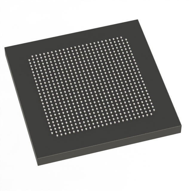
Stratix® V GS Field Programmable Gate Array (FPGA) IC 360 19456000 360000 780-BBGA, FCBGA |
|---|---|
| Quantity | 24 Available (as of June 15, 2026) |

| Product Category | Field Programmable Gate Array (FPGA) |
|---|---|
| Manufacturer | Intel |
| Manufacturing Status | Obsolete |
| Manufacturer Standard Lead Time | Contact Us |
| Datasheet |
Specifications & Environmental
| Device Package | 780-HBGA (33x33) | Grade | Commercial | Operating Temperature | 0°C – 85°C | ||
|---|---|---|---|---|---|---|---|
| Package / Case | 780-BBGA, FCBGA | Number of I/O | 360 | Voltage | 820 mV - 880 mV | ||
| Mounting Method | Surface Mount | RoHS Compliance | RoHS Compliant | REACH Compliance | REACH Unknown | ||
| Moisture Sensitivity Level | 3 (168 Hours) | Number of LABs/CLBs | 135840 | Number of Logic Elements/Cells | 360000 | ||
| Number of Gates | N/A | ECCN | 3A001A2C | HTS Code | 8542.39.0001 | ||
| Qualification | N/A | Total RAM Bits | 19456000 |
Overview of 5SGSMD4E2H29C2L – Stratix® V GS Field Programmable Gate Array (FPGA) IC
The 5SGSMD4E2H29C2L is a Stratix V GS FPGA in a 780-ball BGA (FCBGA) package. It is a high-density, transceiver-capable FPGA offering 360,000 logic elements and abundant DSP and embedded memory resources for data‑intensive, DSP-centric designs.
Designed for applications that require high logic capacity, significant on‑chip memory and variable‑precision DSP, this commercial‑grade device delivers system integration through extensive I/O and advanced fabric features drawn from the Stratix V family architecture.
Key Features
- Logic Capacity — 360,000 logic elements enabling large-scale logic integration and complex RTL implementations.
- Embedded Memory — Approximately 19.5 Mbits of on‑chip RAM (19,456,000 total RAM bits) for buffering, packet storage, and intermediate DSP data.
- DSP Resources — Stratix V GS family variable‑precision DSP blocks; GS devices support up to 3,926 18×18 or 1,963 27×27 multipliers for high‑performance signal processing.
- Transceiver Capability — GS variant includes integrated transceivers with 14.1‑Gbps data‑rate capability for backplane and optical interface applications.
- I/O Density — 360 I/O pins to support complex interfacing and multi‑channel designs.
- Process & Fabric — 28‑nm Stratix V family architecture with redesigned adaptive logic modules (ALMs), multi‑track routing and comprehensive fabric clocking.
- Power Supply — Core supply range specified at 820 mV to 880 mV for this device.
- Package & Mounting — 780‑BBGA (FCBGA), supplier package 780‑HBGA (33×33), surface mount package suitable for high‑density board designs.
- Operating Range — Commercial grade operation from 0 °C to 85 °C; RoHS compliant.
Typical Applications
- High‑performance signal processing — Variable‑precision DSP blocks and abundant multipliers support compute‑intensive DSP workloads and algorithm acceleration.
- Optical and backplane communications — Integrated 14.1‑Gbps transceivers suit backplane and optical interfaces for networking equipment and transport systems.
- Data‑intensive networking — Large logic capacity and embedded memory meet the needs of packet processing, traffic management, and wireline communications systems.
- Broadcast and compute systems — Dense DSP and memory resources enable video processing, encoding/decoding, and other compute‑heavy broadcast applications.
Unique Advantages
- High logic density: 360,000 logic elements allow integration of complex functions and system‑level consolidation on a single device.
- Significant on‑chip memory: Approximately 19.5 Mbits of embedded RAM reduce external memory reliance for buffering and working data storage.
- Rich DSP fabric: Variable‑precision DSP blocks and a large number of multipliers enable flexible, high‑throughput signal processing implementations.
- Transceiver integration: 14.1‑Gbps transceiver capability provides native support for high‑speed serial links and interface lanes.
- Comprehensive I/O: 360 I/O pins support diverse external interfaces and multi‑lane designs without extensive external multiplexing.
- Commercial‑grade reliability: Specified operating range and RoHS compliance for mainstream electronic product deployment.
Why Choose 5SGSMD4E2H29C2L?
This Stratix V GS FPGA delivers a balance of high logic density, ample embedded memory, and a DSP‑focused architecture tailored for transceiver‑centric, data‑intensive applications. Its feature set is suited to engineers building high‑throughput signal processing, networking, broadcast, and compute systems who need on‑chip resources and high‑speed serial capability.
The device leverages Stratix V family fabric innovations—ALMs, M20K memory blocks, PLLs and integrated transceivers—providing a path to consolidate system functions, accelerate algorithms, and reduce external component count while operating within a commercial temperature range.
Request a quote or submit a product inquiry to receive pricing and availability for 5SGSMD4E2H29C2L.


Date Founded: 1968
Headquarters: Santa Clara, California, USA
Employees: 130,000+
Revenue: $54.23 Billion
Certifications and Memberships: ISO9001:2015, ISO14001:2015, ISO17025:2017, ISO27001:2022, ISO45001:2018, ISO50001:2018


