
5SGSMD4E2H29I2L
| Part Description |
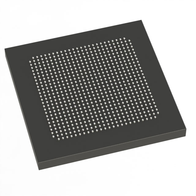
Stratix® V GS Field Programmable Gate Array (FPGA) IC 360 19456000 360000 780-BBGA, FCBGA |
|---|---|
| Quantity | 694 Available (as of June 15, 2026) |

| Product Category | Field Programmable Gate Array (FPGA) |
|---|---|
| Manufacturer | Intel |
| Manufacturing Status | Obsolete |
| Manufacturer Standard Lead Time | Contact Us |
| Datasheet |
Specifications & Environmental
| Device Package | 780-HBGA (33x33) | Grade | Industrial | Operating Temperature | -40°C – 100°C | ||
|---|---|---|---|---|---|---|---|
| Package / Case | 780-BBGA, FCBGA | Number of I/O | 360 | Voltage | 820 mV - 880 mV | ||
| Mounting Method | Surface Mount | RoHS Compliance | RoHS Compliant | REACH Compliance | REACH Unknown | ||
| Moisture Sensitivity Level | 3 (168 Hours) | Number of LABs/CLBs | 135840 | Number of Logic Elements/Cells | 360000 | ||
| Number of Gates | N/A | ECCN | 3A001A2C | HTS Code | 8542.39.0001 | ||
| Qualification | N/A | Total RAM Bits | 19456000 |
Overview of 5SGSMD4E2H29I2L – Stratix® V GS FPGA, 360 I/O, 360,000 logic elements
The 5SGSMD4E2H29I2L is an Intel Stratix V GS field-programmable gate array supplied in a 780-BBGA FCBGA package. It combines a high logic element count with abundant DSP resources, on-chip memory, and integrated transceivers to address bandwidth- and signal-processing‑centric designs.
Designed for industrial-grade applications, this device targets data‑intensive and DSP-oriented systems that require dense logic, extensive I/O, and on‑chip memory while operating across a wide industrial temperature range.
Key Features
- Logic Capacity 360,000 logic elements and 135,840 adaptive logic modules (ALMs) provide high-density programmable fabric for complex designs.
- Embedded Memory Approximately 19.46 Mbits of on‑chip RAM (total RAM bits: 19,456,000) delivered via 20-Kbit (M20K) embedded memory blocks to support large buffers and on-chip data storage.
- DSP Resources Stratix V GS architecture includes a large array of variable-precision DSP blocks; the family supports high-count multipliers for demanding signal-processing tasks.
- High‑speed Transceivers Integrated transceivers with up to 14.1 Gbps capability on GS devices, enabling backplane and optical interface connectivity for high-bandwidth data transport.
- I/O and Packaging 360 user I/Os in a 780‑BBGA FCBGA package (supplier package: 780‑HBGA, 33×33) for dense routing and board-level integration.
- Core Supply Range Core voltage supply range of 820 mV to 880 mV to match system power planning and device requirements.
- Process and Fabric Built on a 28‑nm process with Altera/Intel adaptive logic modules (ALMs) and a multi-track routing architecture for predictable timing and routing resources.
- Industrial Temperature Grade Specified operating temperature from −40 °C to 100 °C for deployment in industrial environments.
- Standards & Compliance RoHS compliant.
Typical Applications
- High‑performance DSP systems Leverage the device’s abundant DSP blocks and on‑chip memory for signal processing, filtering, and algorithm acceleration.
- Optical and backplane interfaces Integrated transceivers support high‑bandwidth serial links for 40G/100G transport and other optical/backplane protocols.
- Packet processing and network equipment Dense logic resources and wide I/O count enable complex packet engines, traffic management, and protocol processing.
- Military, broadcast, and HPC DSP‑centric architectures and robust thermal range make the device suitable for broadcast processing, high‑performance compute, and defense communications.
Unique Advantages
- High logic density: 360,000 logic elements and 135,840 ALMs allow consolidation of large designs into a single device, reducing board count and system complexity.
- Substantial on‑chip memory: Approximately 19.46 Mbits of embedded RAM supports deep buffering and local data storage for latency‑sensitive algorithms.
- DSP‑oriented architecture: Variable‑precision DSP blocks and numerous multipliers accelerate compute‑intensive signal processing without external accelerators.
- Integrated high‑speed I/O: 360 I/Os and transceivers capable of 14.1 Gbps data rates enable high‑bandwidth interfaces directly from the FPGA fabric.
- Industrial robustness: Specified −40 °C to 100 °C operating range and RoHS compliance support deployment in industrial environments.
- Packaging for dense designs: 780‑ball BBGA (33×33) package supports high I/O count and compact PCB implementations.
Why Choose 5SGSMD4E2H29I2L?
The 5SGSMD4E2H29I2L Stratix V GS FPGA balances high logic density, extensive DSP resources, and significant on‑chip memory to address demanding, bandwidth‑ and compute‑intensive applications. Its integrated transceiver capability and large I/O complement systems that require high data throughput and complex protocol handling.
This device is well suited for engineering teams building industrial and high‑performance signal‑processing systems that need a single, scalable FPGA solution with industry‑grade operating range and proven Stratix V architecture characteristics.
Request a quote or submit an inquiry to receive pricing, availability, and lead‑time information for the 5SGSMD4E2H29I2L.


Date Founded: 1968
Headquarters: Santa Clara, California, USA
Employees: 130,000+
Revenue: $54.23 Billion
Certifications and Memberships: ISO9001:2015, ISO14001:2015, ISO17025:2017, ISO27001:2022, ISO45001:2018, ISO50001:2018


