
5SGSMD6N3F45C2N
| Part Description |
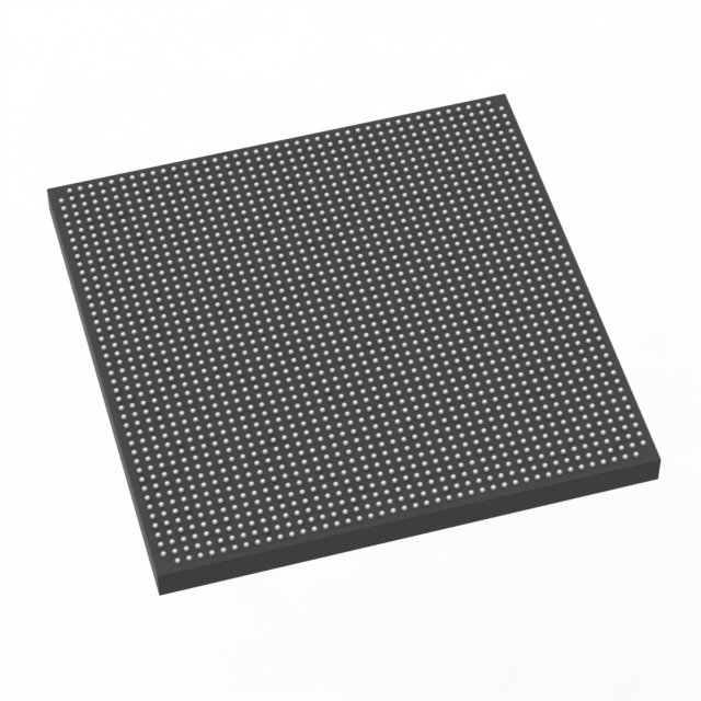
Stratix® V GS Field Programmable Gate Array (FPGA) IC 840 46080000 583000 1932-BBGA, FCBGA |
|---|---|
| Quantity | 1,265 Available (as of June 15, 2026) |

| Product Category | Field Programmable Gate Array (FPGA) |
|---|---|
| Manufacturer | Intel |
| Manufacturing Status | Obsolete |
| Manufacturer Standard Lead Time | Contact Us |
| Datasheet |
Specifications & Environmental
| Device Package | 1932-FBGA, FC (45x45) | Grade | Commercial | Operating Temperature | 0°C – 85°C | ||
|---|---|---|---|---|---|---|---|
| Package / Case | 1932-BBGA, FCBGA | Number of I/O | 840 | Voltage | 870 mV - 930 mV | ||
| Mounting Method | Surface Mount | RoHS Compliance | RoHS Compliant | REACH Compliance | REACH Unknown | ||
| Moisture Sensitivity Level | 3 (168 Hours) | Number of LABs/CLBs | 220000 | Number of Logic Elements/Cells | 583000 | ||
| Number of Gates | N/A | ECCN | 3A001A2C | HTS Code | 8542.39.0001 | ||
| Qualification | N/A | Total RAM Bits | 46080000 |
Overview of 5SGSMD6N3F45C2N – Stratix® V GS FPGA, 583,000 logic elements
The 5SGSMD6N3F45C2N is a Stratix® V GS field programmable gate array (FPGA) packaged in a high-pin-count FCBGA. It provides a large programmable fabric with high I/O capacity and substantial on-chip memory for complex digital designs. Typical use cases include systems that require dense logic consolidation, extensive I/O connectivity, and significant embedded memory resources.
Key Features
- Logic Capacity 583,000 logic elements and approximately 220,000 logic array blocks provide high-density programmable logic for complex function implementation.
- Embedded Memory Approximately 46 Mbits of total on-chip RAM to support buffering, FIFOs, and lookup tables without external memory.
- I/O Resources 840 user I/Os to support wide parallel interfaces and high-pin-count system integration.
- Power Core supply voltage specified between 870 mV and 930 mV for the programmable fabric.
- Package & Mounting 1932-BBGA (FCBGA, 45 × 45) package in a surface-mount form factor designed for dense board-level integration.
- Temperature & Grade Commercial grade device with an operating temperature range of 0 °C to 85 °C.
- Environmental Compliance RoHS compliant.
Typical Applications
- High-density digital systems Use the large logic capacity and embedded RAM to consolidate multiple functions into a single, reconfigurable device.
- Data buffering and packet processing Leverage the approximately 46 Mbits of on-chip RAM and abundant I/Os for packet buffering, queues, and intermediate storage.
- Multi-I/O interface hubs The 840 I/Os enable complex board-level interfacing, bridging, and protocol adaptation tasks that need many parallel connections.
- Prototyping and system validation Dense logic and large I/O count allow rapid hardware prototyping of system-level designs within a commercial temperature envelope.
Unique Advantages
- High logic density: 583,000 logic elements let you implement large, partitioned designs without immediate external decomposition.
- Substantial on-chip RAM: Approximately 46 Mbits of embedded memory reduces dependence on off-chip memory for many buffering and storage tasks.
- Extensive I/O capability: 840 I/Os facilitate broad connectivity for multi-channel and parallel-interface applications, minimizing glue logic.
- High-pin-count FCBGA package: The 1932-BBGA (45 × 45) package supports complex PCB routing and dense system integrations.
- Commercial temperature suitability: Rated for 0 °C to 85 °C to match a wide range of commercial electronic applications.
- RoHS compliant: Environmentally compliant for deployment in lead-free manufacturing flows.
Why Choose 5SGSMD6N3F45C2N?
The 5SGSMD6N3F45C2N combines high logic element count, large embedded memory, and a very high I/O count in a single Stratix V GS FCBGA package, making it suitable for dense, I/O-heavy designs in commercial-temperature applications. Its core voltage range and surface-mount FCBGA packaging support modern board-level integration and power architectures.
This device is well suited to engineers and procurement teams specifying FPGA solutions that require consolidated logic, on-chip buffering, and broad connectivity while maintaining RoHS compliance and commercial-grade operating conditions.
Request a quote or submit an inquiry for pricing and lead-time information to move this FPGA into your BOM and project schedule.


Date Founded: 1968
Headquarters: Santa Clara, California, USA
Employees: 130,000+
Revenue: $54.23 Billion
Certifications and Memberships: ISO9001:2015, ISO14001:2015, ISO17025:2017, ISO27001:2022, ISO45001:2018, ISO50001:2018


