
5SGSMD8N2F45I2LN
| Part Description |
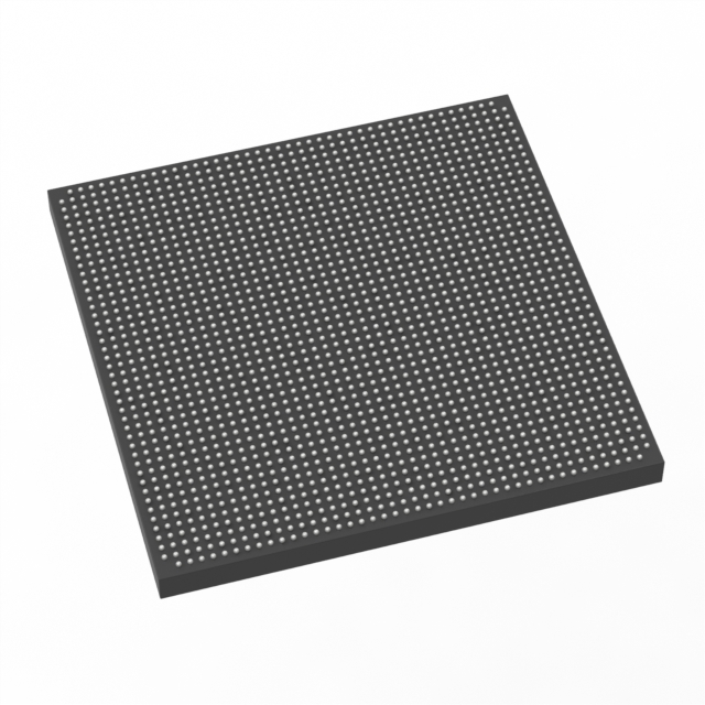
Stratix® V GS Field Programmable Gate Array (FPGA) IC 840 51200000 695000 1932-BBGA, FCBGA |
|---|---|
| Quantity | 724 Available (as of June 10, 2026) |

| Product Category | Field Programmable Gate Array (FPGA) |
|---|---|
| Manufacturer | Intel |
| Manufacturing Status | Obsolete |
| Manufacturer Standard Lead Time | Contact Us |
| Datasheet |
Specifications & Environmental
| Device Package | 1932-FBGA, FC (45x45) | Grade | Industrial | Operating Temperature | -40°C – 100°C | ||
|---|---|---|---|---|---|---|---|
| Package / Case | 1932-BBGA, FCBGA | Number of I/O | 840 | Voltage | 820 mV - 880 mV | ||
| Mounting Method | Surface Mount | RoHS Compliance | RoHS Compliant | REACH Compliance | REACH Unknown | ||
| Moisture Sensitivity Level | 3 (168 Hours) | Number of LABs/CLBs | 262400 | Number of Logic Elements/Cells | 695000 | ||
| Number of Gates | N/A | ECCN | 3A001A2C | HTS Code | 8542.39.0001 | ||
| Qualification | N/A | Total RAM Bits | 51200000 |
Overview of 5SGSMD8N2F45I2LN – Stratix® V GS Field Programmable Gate Array (FPGA) IC
The 5SGSMD8N2F45I2LN is a Stratix V GS family FPGA offering high logic capacity and on-chip memory for industrial applications. As a high-density, industrial-grade FPGA in a 1932-BBGA FCBGA package, it targets designs that require substantial logic resources, extensive I/O, and operation across a wide temperature range.
With 695,000 logic elements, approximately 51.2 Mbits of embedded RAM, and 840 user I/Os, this device is engineered to deliver large-scale integration and system consolidation while operating from a core voltage range of 820 mV to 880 mV.
Key Features
- Logic Capacity 695,000 logic elements provide a large fabric for implementing complex custom logic, datapaths, and state machines.
- Logic Blocks 262,400 logic blocks support hierarchical design and resource partitioning for large designs.
- Embedded Memory Approximately 51.2 Mbits of on-chip RAM enables large buffers, FIFOs, and on-chip data storage without external memory dependence.
- I/O Count 840 user I/Os accommodate wide parallel interfaces, multiple high-pin-count peripherals, and flexible board-level routing.
- Power and Core Voltage Core supply range of 820 mV to 880 mV supports operation within defined low-voltage FPGA core requirements.
- Package and Mounting 1932-BBGA (FCBGA, 45×45) surface-mount package provides a high-pin-count footprint suitable for dense interconnect on multi-layer PCBs.
- Industrial Temperature Grade Rated for operation from −40 °C to 100 °C to meet industrial-environment requirements.
- Regulatory RoHS compliant for lead-free assembly processes and environmental compliance.
Typical Applications
- Industrial Control Systems Implements complex control algorithms and large I/O interfacing where wide temperature range and high logic density are required.
- Data Processing and Acceleration Hosts large-scale datapaths and on-chip buffering using substantial logic resources and embedded RAM for low-latency processing.
- Communications Infrastructure Supports dense I/O and integration of protocol and framing logic for network and telecom equipment.
- Test & Measurement Equipment Enables custom signal conditioning, aggregation, and deterministic logic timing in industrial test systems.
Unique Advantages
- High integration density: 695,000 logic elements and ~51.2 Mbits of embedded RAM reduce the need for external components and simplify system BOM.
- Extensive I/O capability: 840 user I/Os allow direct interfacing to multiple peripherals and high-pin-count connectors without external multiplexing.
- Industrial robustness: Specified for −40 °C to 100 °C operation to meet demanding environmental conditions in industrial deployments.
- Compact, high-pin-count package: 1932-BBGA (FCBGA) delivers dense routing and signal integrity advantages for complex PCB designs.
- Controlled core supply: Narrow core voltage range (820–880 mV) supports predictable power design and thermal planning.
- RoHS compliant: Facilitates lead-free manufacturing and compliance with environmental regulations.
Why Choose 5SGSMD8N2F45I2LN?
The 5SGSMD8N2F45I2LN positions itself as a high-capacity, industrial-grade FPGA suitable for designs that demand large programmable logic fabrics, substantial on-chip memory, and broad I/O resources. Its combination of logic density, embedded RAM, and an extensive I/O set makes it well suited for consolidation of complex systems onto a single programmable device.
For engineering teams building industrial controls, communications equipment, or high-performance processing modules, this Stratix V GS device offers scalable resources, predictable operating voltage requirements, and a package tailored for high-pin-count board layouts—supporting long-term design stability and manufacturability.
Request a quote or submit an inquiry to obtain pricing, lead-time, and availability for the 5SGSMD8N2F45I2LN.


Date Founded: 1968
Headquarters: Santa Clara, California, USA
Employees: 130,000+
Revenue: $54.23 Billion
Certifications and Memberships: ISO9001:2015, ISO14001:2015, ISO17025:2017, ISO27001:2022, ISO45001:2018, ISO50001:2018


