
5SGXEA3K3F40C2LG
| Part Description |
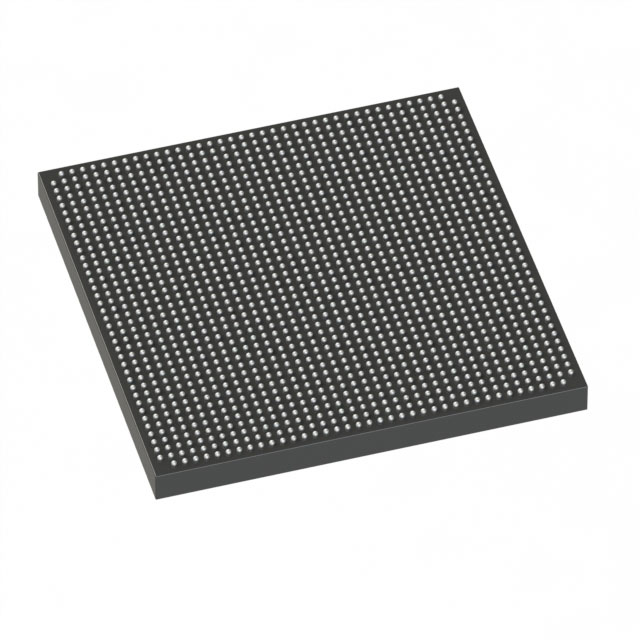
Stratix® V GX Field Programmable Gate Array (FPGA) IC 696 19456000 340000 1517-BBGA, FCBGA |
|---|---|
| Quantity | 579 Available (as of June 15, 2026) |

| Product Category | Field Programmable Gate Array (FPGA) |
|---|---|
| Manufacturer | Intel |
| Manufacturing Status | Active |
| Manufacturer Standard Lead Time | 26 Weeks |
| Datasheet |
Specifications & Environmental
| Device Package | 1517-FBGA (40x40) | Grade | Commercial | Operating Temperature | 0°C – 85°C | ||
|---|---|---|---|---|---|---|---|
| Package / Case | 1517-BBGA, FCBGA | Number of I/O | 696 | Voltage | 820 mV - 880 mV | ||
| Mounting Method | Surface Mount | RoHS Compliance | RoHS Compliant | REACH Compliance | REACH Unaffected | ||
| Moisture Sensitivity Level | 3 (168 Hours) | Number of LABs/CLBs | 128300 | Number of Logic Elements/Cells | 340000 | ||
| Number of Gates | N/A | ECCN | N/A | HTS Code | N/A | ||
| Qualification | N/A | Total RAM Bits | 19456000 |
Overview of 5SGXEA3K3F40C2LG – Stratix® V GX FPGA, 1517-BBGA, 696 I/Os
The 5SGXEA3K3F40C2LG is a Stratix V GX field programmable gate array (FPGA) in a 1517‑BBGA FCBGA package. It delivers a large programmable fabric with a high I/O count and significant on‑chip memory for complex digital designs.
Designed for commercial applications, this device targets high‑density logic integration, memory‑intensive functions, and systems requiring substantial I/O connectivity while operating within a 0 °C to 85 °C temperature range.
Key Features
- High Logic Capacity Approximately 340,000 logic elements to implement large-scale digital logic and custom accelerators.
- Embedded Memory Approximately 19.456 Mbits of on‑chip RAM for buffering, packet processing, and temporary storage.
- Extensive I/O 696 general-purpose I/Os to support high‑channel count interfaces and parallel connectivity.
- Package and Mounting 1517‑BBGA (FCBGA) package; supplier device package noted as 1517‑FBGA (40×40). Surface‑mount mounting type for standard board assembly.
- Power Voltage supply range of 820 mV to 880 mV, consistent with low‑voltage FPGA core operation.
- Commercial Grade Specified for commercial temperature operation from 0 °C to 85 °C.
- Environmental Compliance RoHS compliant.
- Series Transceiver Capability (series level) The Stratix V GX family (series-level information) includes GX transceiver speed grades; see series documentation for available transceiver options and speed grades.
Typical Applications
- High‑density logic acceleration Use the device's ~340,000 logic elements to implement custom accelerators, data path engines, and compute offload functions.
- Memory‑intensive processing Leverage approximately 19.456 Mbits of embedded RAM for buffering, packet queues, and on‑chip data staging.
- High‑channel I/O aggregation Deploy the 696 I/Os for multiport communications, large sensor arrays, or high‑channel control systems.
- Communications and protocol bridging Combine the device's logic capacity and I/O density to implement protocol conversion, interface bridging, and system glue logic (refer to series documentation for transceiver options).
Unique Advantages
- High logic density: The large logic element count enables implementation of complex, consolidated designs that reduce the need for multiple devices.
- Substantial on‑chip memory: Approximately 19.456 Mbits of embedded RAM reduces external memory dependencies for many buffering and queuing tasks.
- Massive I/O capacity: 696 I/Os allow direct connection to numerous peripherals, sensors, and parallel interfaces without extensive external multiplexing.
- Compact FCBGA package: The 1517‑BBGA (1517‑FBGA supplier package, 40×40) provides a high–pin‑count solution in a board‑space efficient footprint.
- Low‑voltage core operation: Core supply range (820 mV–880 mV) aligns with modern low‑power FPGA core requirements.
- Commercial qualification and RoHS compliance: Commercial temperature grade (0 °C–85 °C) and RoHS compliance support mainstream product deployments and regulatory needs.
Why Choose 5SGXEA3K3F40C2LG?
This Stratix V GX device combines large programmable logic capacity, ample embedded memory, and one of the highest I/O counts in its package class to address demanding commercial designs that require integration of complex logic, local storage, and extensive interfacing. Its surface‑mount FCBGA package and documented operating range make it suitable for production systems where board‑level integration density and predictable electrical characteristics are important.
Engineers designing high‑performance communications, compute acceleration, or multiport I/O systems will find the 5SGXEA3K3F40C2LG appropriate for consolidating functionality, reducing BOM complexity, and enabling compact implementations while relying on series documentation for transceiver and family‑level details.
Request a quote or submit an inquiry to get pricing and availability for the 5SGXEA3K3F40C2LG.


Date Founded: 1968
Headquarters: Santa Clara, California, USA
Employees: 130,000+
Revenue: $54.23 Billion
Certifications and Memberships: ISO9001:2015, ISO14001:2015, ISO17025:2017, ISO27001:2022, ISO45001:2018, ISO50001:2018


