
5SGXEA4K2F35C2N
| Part Description |
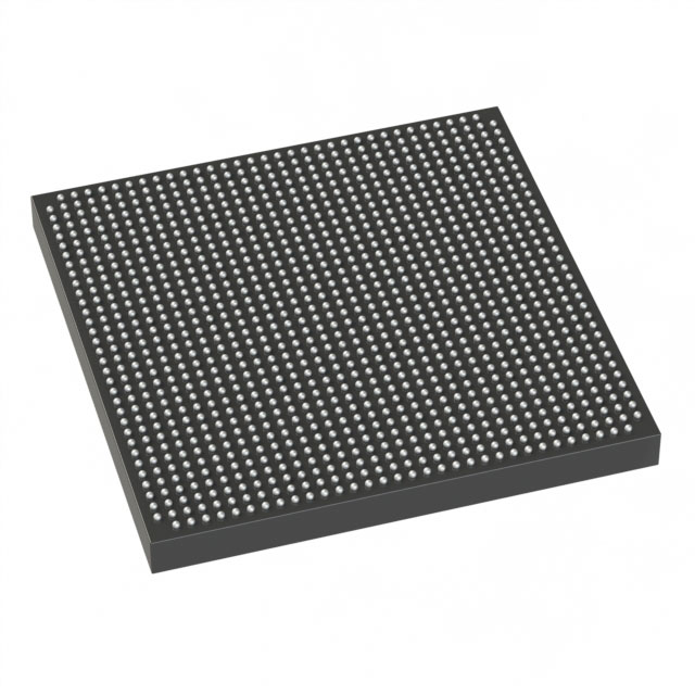
Stratix® V GX Field Programmable Gate Array (FPGA) IC 432 37888000 420000 1152-BBGA, FCBGA |
|---|---|
| Quantity | 449 Available (as of June 10, 2026) |

| Product Category | Field Programmable Gate Array (FPGA) |
|---|---|
| Manufacturer | Intel |
| Manufacturing Status | Obsolete |
| Manufacturer Standard Lead Time | Contact Us |
| Datasheet |
Specifications & Environmental
| Device Package | 1152-FBGA (35x35) | Grade | Commercial | Operating Temperature | 0°C – 85°C | ||
|---|---|---|---|---|---|---|---|
| Package / Case | 1152-BBGA, FCBGA | Number of I/O | 432 | Voltage | 870 mV - 930 mV | ||
| Mounting Method | Surface Mount | RoHS Compliance | RoHS Compliant | REACH Compliance | REACH Unknown | ||
| Moisture Sensitivity Level | 3 (168 Hours) | Number of LABs/CLBs | 158500 | Number of Logic Elements/Cells | 420000 | ||
| Number of Gates | N/A | ECCN | 3A001A2C | HTS Code | 8542.39.0001 | ||
| Qualification | N/A | Total RAM Bits | 37888000 |
Overview of 5SGXEA4K2F35C2N – Stratix® V GX Field Programmable Gate Array (FPGA), 420000 logic elements, ~38 Mbits RAM, 432 I/Os
The 5SGXEA4K2F35C2N is a Stratix® V GX field programmable gate array (FPGA) IC provided in a 1152-BBGA (35 × 35 mm) FCBGA package for surface-mount applications. The device offers 420,000 logic elements and approximately 38 Mbits of embedded memory, together with 432 general-purpose I/Os and Stratix V GX family electrical and switching characteristics documented in the device datasheet.
Designed for commercial-temperature applications (0 °C to 85 °C), this part operates with a core supply in the 870 mV to 930 mV range and is supplied in a 1152-FBGA package format. The Stratix V GX family datasheet provides detailed electrical and transceiver-related characteristics relevant to integration and system design.
Key Features
- Core and Logic 420,000 logic elements suitable for high-density programmable logic implementations.
- Embedded Memory Approximately 38 Mbits of on-chip RAM for buffering, state storage, and data-path implementations.
- I/O and Periphery 432 device I/Os to support extensive external connectivity and system interfacing.
- Package and Mounting 1152-BBGA (FCBGA) supplier package (1152-FBGA, 35 × 35 mm) with surface-mount mounting for compact board-level integration.
- Power Core voltage supply range of 870 mV to 930 mV, enabling design alignment with specified power rails.
- Operating Conditions Commercial-grade operation across 0 °C to 85 °C as specified for the device.
- Standards and Documentation Device electrical and switching characteristics, including I/O timing and transceiver information, are described in the Stratix V device datasheet.
- Regulatory Status RoHS compliant.
Typical Applications
- High-density digital processing Implement compute-intensive, logic-rich functions using the device’s 420,000 logic elements and significant on-chip RAM.
- Embedded memory–dependent designs Use the approximately 38 Mbits of embedded memory for buffering, FIFOs, and intermediate data storage inside the FPGA fabric.
- High I/O connectivity systems Leverage 432 I/Os for multi-channel connectivity, control-plane interfaces, and broad peripheral integration.
- FPGA-based development and prototyping Employ the Stratix V GX device and its documented electrical characteristics for system-level validation and functional prototyping.
Unique Advantages
- Large logic capacity: 420,000 logic elements provide substantial programmable resources for complex designs.
- Significant on-chip RAM: Approximately 38 Mbits of embedded memory reduces external memory dependencies for many use cases.
- High I/O count: 432 I/Os enable broad external interfacing and flexible board-level connectivity.
- Compact FCBGA package: 1152-BBGA (35 × 35 mm) package allows dense board integration while maintaining the available I/O and logic resources.
- Commercial-temperature qualification: Rated for 0 °C to 85 °C operation to support standard commercial applications.
- Datasheet-backed specifications: Electrical, switching, I/O timing, and transceiver details are documented in the Stratix V device datasheet for design validation.
Why Choose 5SGXEA4K2F35C2N?
The 5SGXEA4K2F35C2N combines high logic density, substantial embedded memory, and a large I/O complement in a compact 1152-BBGA FCBGA package. Its documented Stratix V GX electrical and switching characteristics support design decisions where on-chip resources and verified I/O behavior are required.
This part is suited for teams and designs that require dense programmable logic, significant on-chip RAM, and extensive I/O in a commercial-temperature device. The combination of these measurable specifications supports scalable implementations and system integration backed by the Stratix V device documentation.
Request a quote or submit an inquiry to purchase the 5SGXEA4K2F35C2N and receive pricing and availability information for your design requirements.


Date Founded: 1968
Headquarters: Santa Clara, California, USA
Employees: 130,000+
Revenue: $54.23 Billion
Certifications and Memberships: ISO9001:2015, ISO14001:2015, ISO17025:2017, ISO27001:2022, ISO45001:2018, ISO50001:2018


