
5SGXEA5H2F35C2N
| Part Description |
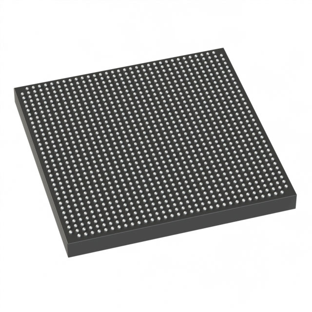
Stratix® V GX Field Programmable Gate Array (FPGA) IC 552 46080000 490000 1152-BBGA, FCBGA |
|---|---|
| Quantity | 530 Available (as of June 10, 2026) |
| Product Category | Field Programmable Gate Array (FPGA) |
|---|---|
| Manufacturer | Intel |
| Manufacturing Status | Obsolete |
| Manufacturer Standard Lead Time | Contact Us |
| Datasheet |
Specifications & Environmental
| Device Package | 1152-FBGA (35x35) | Grade | Commercial | Operating Temperature | 0°C – 85°C | ||
|---|---|---|---|---|---|---|---|
| Package / Case | 1152-BBGA, FCBGA | Number of I/O | 552 | Voltage | 870 mV - 930 mV | ||
| Mounting Method | Surface Mount | RoHS Compliance | RoHS Compliant | REACH Compliance | REACH Unknown | ||
| Moisture Sensitivity Level | 3 (168 Hours) | Number of LABs/CLBs | 185000 | Number of Logic Elements/Cells | 490000 | ||
| Number of Gates | N/A | ECCN | 3A001A2C | HTS Code | 8542.39.0001 | ||
| Qualification | N/A | Total RAM Bits | 46080000 |
Overview of 5SGXEA5H2F35C2N – Stratix® V GX FPGA, 1152-FBGA (35×35)
The 5SGXEA5H2F35C2N is a Stratix® V GX field programmable gate array (FPGA) in a 1152-ball FCBGA package optimized for high-density, programmable digital logic. It delivers a large logic fabric and on-chip memory with a high I/O count and a low-voltage core supply, making it suitable for designs that require concentrated logic capacity and extensive peripheral interfacing.
The device follows the Stratix V family electrical and switching characteristics described in the device datasheet, including core and periphery performance and transceiver-related specifications for GX-class devices.
Key Features
- Logic Capacity Approximately 490,000 logic elements for large-scale programmable logic integration and complex designs.
- Embedded Memory Approximately 46 Mbits of on-chip RAM to support buffering, lookup tables, and data storage within the FPGA fabric.
- I/O Resources 552 user I/O pins to support broad peripheral connectivity and multiple interface implementations.
- Package & Mounting 1152-ball FBGA (35×35 mm) package, surface-mountable for compact board-level integration.
- Power Core supply range of 870 mV to 930 mV to match low-voltage system designs.
- Temperature & Grade Commercial grade with an operating range of 0 °C to 85 °C.
- Regulatory RoHS-compliant for regulatory and environmental compatibility.
- Family-Level Documentation Datasheet coverage includes electrical and switching characteristics, I/O timing, and transceiver information relevant to Stratix V GX devices.
Typical Applications
- Custom digital logic Implement complex, application-specific logic functions and state machines using the device's high logic and memory resources.
- High-density system integration Consolidate multiple functions into a single FPGA to reduce component count and simplify board design.
- High-pin-count interfacing Support extensive peripheral and interface routing with 552 I/O pins for flexible system connectivity.
- Prototyping and development Leverage the programmable fabric and on-chip memory for rapid prototyping and iterative hardware development.
Unique Advantages
- High logic capacity: The device’s approximately 490,000 logic elements enable complex designs and feature-rich implementations.
- Substantial embedded memory: Approximately 46 Mbits of on-chip RAM reduces the need for external memory for many buffering and storage tasks.
- Broad I/O availability: 552 I/O pins provide flexibility for interfacing to multiple peripherals and external devices without external expanders.
- Compact, surface-mount package: The 1152-FBGA (35×35) package supports high-density PCB layouts while maintaining strong thermal and electrical characteristics.
- Low-voltage core: Core operation in the 870 mV to 930 mV range supports integration into low-voltage system power architectures.
- Commercial temperature rating: Designed for 0 °C to 85 °C operation, suitable for a wide range of commercial electronic applications.
Why Choose 5SGXEA5H2F35C2N?
The 5SGXEA5H2F35C2N positions itself as a high-density Stratix V GX FPGA option that combines substantial logic and embedded memory with a large I/O complement and a compact FBGA package. It is well suited to designers needing to consolidate complex digital functions, build high-pin-count interfaces, or accelerate development with a programmable platform.
Backed by the Stratix V GX family documentation from the manufacturer, this device provides measurable specifications for electrical and switching characteristics that help engineers evaluate system-level performance and integration trade-offs during design and validation.
Request a quote or submit an inquiry to obtain pricing, availability, and lead-time information for the 5SGXEA5H2F35C2N.


Date Founded: 1968
Headquarters: Santa Clara, California, USA
Employees: 130,000+
Revenue: $54.23 Billion
Certifications and Memberships: ISO9001:2015, ISO14001:2015, ISO17025:2017, ISO27001:2022, ISO45001:2018, ISO50001:2018


