
5SGXEA5H2F35C2G
| Part Description |
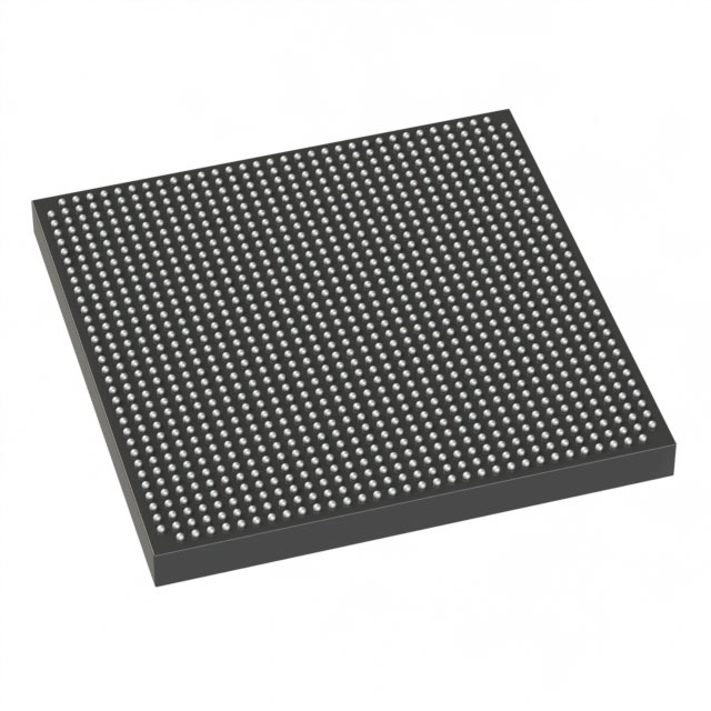
Stratix® V GX Field Programmable Gate Array (FPGA) IC 552 46080000 490000 1152-BBGA, FCBGA |
|---|---|
| Quantity | 204 Available (as of June 15, 2026) |

| Product Category | Field Programmable Gate Array (FPGA) |
|---|---|
| Manufacturer | Intel |
| Manufacturing Status | Active |
| Manufacturer Standard Lead Time | 26 Weeks |
| Datasheet |
Specifications & Environmental
| Device Package | 1152-FBGA (35x35) | Grade | Commercial | Operating Temperature | 0°C – 85°C | ||
|---|---|---|---|---|---|---|---|
| Package / Case | 1152-BBGA, FCBGA | Number of I/O | 552 | Voltage | 870 mV - 930 mV | ||
| Mounting Method | Surface Mount | RoHS Compliance | RoHS Compliant | REACH Compliance | REACH Unaffected | ||
| Moisture Sensitivity Level | 3 (168 Hours) | Number of LABs/CLBs | 185000 | Number of Logic Elements/Cells | 490000 | ||
| Number of Gates | N/A | ECCN | N/A | HTS Code | N/A | ||
| Qualification | N/A | Total RAM Bits | 46080000 |
Overview of 5SGXEA5H2F35C2G – Stratix® V GX FPGA, 490,000 logic elements, ~46.08 Mbits RAM, 552 I/Os
The 5SGXEA5H2F35C2G is a Stratix V GX Field Programmable Gate Array (FPGA) IC in a 1152-ball FCBGA/FBGA package. It provides a high-density, commercial‑grade programmable logic platform with substantial on-chip memory and a large I/O complement for complex system designs.
Key device-level specifications include approximately 490,000 logic elements, roughly 46.08 Mbits of embedded RAM, 552 user I/Os, and a supply-voltage operating window of 870 mV to 930 mV. As part of the Stratix V GX family, the device series includes high‑speed transceiver speed grades (up to 14.1 Gbps at the family level, per device datasheet).
Key Features
- Core Logic Approximately 490,000 logic elements to implement large, complex FPGA designs and deep datapaths.
- Embedded Memory Approximately 46.08 Mbits of on‑chip RAM for buffering, LUT storage, and intermediate data processing.
- I/O Capacity 552 user I/Os providing extensive external connectivity and interface flexibility for multi‑lane and multi‑device systems.
- High‑Speed Transceivers (family‑level) Stratix V GX devices support transceiver speed grades up to 14.1 Gbps (refer to Stratix V device documentation for specific speed‑grade options and channel capabilities).
- Power and Supply Core supply range specified at 870 mV to 930 mV for predictable power domain planning.
- Package & Mounting 1152-ball FBGA/BBGA (35 × 35) FCBGA package for surface‑mount PCB assembly and high‑density board integration.
- Commercial Temperature Grade Specified operating temperature range of 0 °C to 85 °C for commercial applications.
- Regulatory RoHS compliant.
Typical Applications
- High‑performance networking and communications Large logic capacity, abundant I/Os, and Stratix V GX transceiver capabilities support protocol processing, packet routing, and multi‑lane interfaces.
- Data processing and acceleration Extensive logic resources and embedded RAM enable custom acceleration, compute offload, and complex dataflow implementations.
- Signal processing and instrumentation High on‑chip memory and many I/Os facilitate real‑time aggregation, buffering, and processing of high‑bandwidth signals.
- Board‑level integration The 1152‑ball FCBGA package and large I/O count simplify integration in dense, multi‑layer PCB designs.
Unique Advantages
- Highly integrated logic and memory: The combination of roughly 490,000 logic elements and ~46.08 Mbits of embedded RAM reduces reliance on external memory and simplifies system architecture.
- Large I/O surface for system interfacing: 552 user I/Os allow flexible, high‑pincount connectivity for multi‑interface systems and parallel data paths.
- Family‑level high‑speed serial capability: Stratix V GX transceiver speed grades (up to 14.1 Gbps at the family level) provide options for high‑bandwidth serial links where required.
- Commercial temperature rating: Clear 0 °C to 85 °C rating supports mainstream commercial deployments and predictable thermal design.
- Proven documentation and device characterization: Electrical and switching characteristics for the Stratix V family are documented in the device datasheet, aiding design verification and system qualification.
- RoHS compliant: Aligns with common environmental and manufacturing requirements.
Why Choose 5SGXEA5H2F35C2G?
The 5SGXEA5H2F35C2G delivers a high‑density, commercially rated Stratix V GX FPGA option for engineers building complex, high‑bandwidth systems that require extensive logic, significant on‑chip memory, and a large number of I/Os. Its package and supply specifications make it suitable for dense board integration and commercial applications where documented device behavior and family‑level transceiver options are important.
This device is well suited to teams implementing protocol processing, data acceleration, and high‑throughput signal processing who depend on documented device characteristics from the Stratix V family to plan power, thermal, and I/O architectures.
If you would like pricing, availability, or a quote for 5SGXEA5H2F35C2G, request a quote or contact sales to discuss your project requirements and lead times.


Date Founded: 1968
Headquarters: Santa Clara, California, USA
Employees: 130,000+
Revenue: $54.23 Billion
Certifications and Memberships: ISO9001:2015, ISO14001:2015, ISO17025:2017, ISO27001:2022, ISO45001:2018, ISO50001:2018


