
5SGXEA5H2F35C1G
| Part Description |
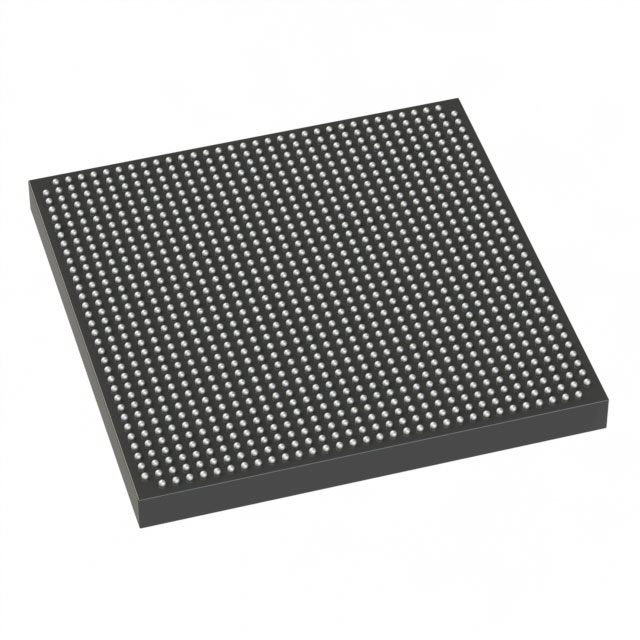
Stratix® V GX Field Programmable Gate Array (FPGA) IC 552 46080000 490000 1152-BBGA, FCBGA |
|---|---|
| Quantity | 358 Available (as of June 10, 2026) |
| Product Category | Field Programmable Gate Array (FPGA) |
|---|---|
| Manufacturer | Intel |
| Manufacturing Status | Active |
| Manufacturer Standard Lead Time | 26 Weeks |
| Datasheet |
Specifications & Environmental
| Device Package | 1152-FBGA (35x35) | Grade | Commercial | Operating Temperature | 0°C – 85°C | ||
|---|---|---|---|---|---|---|---|
| Package / Case | 1152-BBGA, FCBGA | Number of I/O | 552 | Voltage | 870 mV - 930 mV | ||
| Mounting Method | Surface Mount | RoHS Compliance | RoHS Compliant | REACH Compliance | REACH Unaffected | ||
| Moisture Sensitivity Level | 3 (168 Hours) | Number of LABs/CLBs | 185000 | Number of Logic Elements/Cells | 490000 | ||
| Number of Gates | N/A | ECCN | N/A | HTS Code | N/A | ||
| Qualification | N/A | Total RAM Bits | 46080000 |
Overview of 5SGXEA5H2F35C1G – Stratix® V GX FPGA, 490,000 logic elements, ~46 Mbits RAM, 552 I/O, 1152-FBGA
The 5SGXEA5H2F35C1G is a Stratix V GX field programmable gate array (FPGA) in a high-density FCBGA package. It provides a large logic capacity and substantial on-chip memory for complex, custom digital designs.
Designed for applications that require high logic element counts, significant embedded RAM, and extensive I/O, this commercial-grade device balances performance and integration with a low-voltage core operating range and RoHS compliance.
Key Features
- Core Logic — 490,000 logic elements suitable for large-scale custom logic implementations and complex combinational/sequential designs.
- Embedded Memory — Approximately 46 Mbits of on-chip RAM to support buffering, large state machines, and memory-intensive algorithms.
- I/O Density — 552 user I/O pins to support multiple high-pin-count interfaces and board-level integration.
- Package & Mounting — 1152-FBGA (35×35) package case in a surface-mount FCBGA form factor for high-density PCB assembly.
- Power — Core voltage supply range of 870 mV to 930 mV, enabling low-voltage operation for the device core.
- Grade & Temperature — Commercial grade with an operating temperature range of 0°C to 85°C.
- Regulatory — RoHS compliant for environmental and manufacturing compatibility.
Typical Applications
- High-density signal processing — Large logic capacity and on-chip RAM support complex DSP pipelines and custom data-path implementations.
- High-pin-count interface hubs — 552 I/O enable aggregation and bridging of multiple board-level interfaces and peripherals.
- Compute acceleration and prototyping — Substantial logic and memory resources make it suitable for hardware acceleration prototypes and large custom accelerators.
- Complex control systems — Ample logic elements and embedded RAM allow implementation of advanced control algorithms and state-machine intensive designs.
Unique Advantages
- High logic density: 490,000 logic elements provide extensive capacity for integrating large amounts of bespoke logic on a single device.
- Significant embedded memory: Approximately 46 Mbits of on-chip RAM reduce dependency on external memory for many buffering and state-storage needs.
- Extensive I/O: 552 user I/O pins simplify system integration where multiple interfaces or parallel connections are required.
- Compact, high-pin-count package: The 1152-FBGA (35×35) FCBGA package supports dense PCB layouts while maintaining broad routing capability.
- Low-voltage core operation: Core supply range of 870–930 mV supports designs optimized for lower-power core operation.
- Commercial readiness: Rated for 0°C to 85°C operation and RoHS compliant for mainstream commercial products.
Why Choose 5SGXEA5H2F35C1G?
This Stratix V GX device is positioned for designs that need a combination of very high logic capacity, substantial embedded RAM, and a large number of I/O signals in a compact FCBGA package. Its electrical characteristics and package make it suitable for complex FPGA-based systems where integration density and on-chip memory are key design drivers.
For engineering teams and procurement looking to scale prototypes into production-ready commercial designs, the 5SGXEA5H2F35C1G offers a balance of integration, thermal-operating range, and regulatory compliance that supports long-term design stability and supply-chain compatibility.
Request a quote or submit an inquiry for pricing and availability of the 5SGXEA5H2F35C1G to evaluate it for your next high-density FPGA design.


Date Founded: 1968
Headquarters: Santa Clara, California, USA
Employees: 130,000+
Revenue: $54.23 Billion
Certifications and Memberships: ISO9001:2015, ISO14001:2015, ISO17025:2017, ISO27001:2022, ISO45001:2018, ISO50001:2018


