
5SGXEA7H2F35C1N
| Part Description |
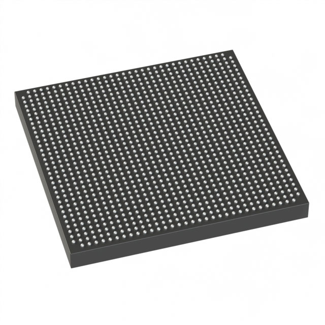
Stratix® V GX Field Programmable Gate Array (FPGA) IC 552 51200000 622000 1152-BBGA, FCBGA |
|---|---|
| Quantity | 820 Available (as of June 10, 2026) |

| Product Category | Field Programmable Gate Array (FPGA) |
|---|---|
| Manufacturer | Intel |
| Manufacturing Status | Obsolete |
| Manufacturer Standard Lead Time | Contact Us |
| Datasheet |
Specifications & Environmental
| Device Package | 1152-FBGA (35x35) | Grade | Commercial | Operating Temperature | 0°C – 85°C | ||
|---|---|---|---|---|---|---|---|
| Package / Case | 1152-BBGA, FCBGA | Number of I/O | 552 | Voltage | 870 mV - 930 mV | ||
| Mounting Method | Surface Mount | RoHS Compliance | RoHS Compliant | REACH Compliance | REACH Unknown | ||
| Moisture Sensitivity Level | 3 (168 Hours) | Number of LABs/CLBs | 234720 | Number of Logic Elements/Cells | 622000 | ||
| Number of Gates | N/A | ECCN | 3A001A2C | HTS Code | 8542.39.0001 | ||
| Qualification | N/A | Total RAM Bits | 51200000 |
Overview of 5SGXEA7H2F35C1N – Stratix® V GX FPGA, 622,000 Logic Elements, 51.2 Mbit RAM, 552 I/Os
The 5SGXEA7H2F35C1N is a Stratix® V GX field programmable gate array (FPGA) from Intel. It provides a high-density programmable fabric with substantial on‑chip memory and a large I/O count to support complex digital designs.
Built for commercial-grade applications, this device delivers approximately 622,000 logic elements, roughly 51.2 Mbits of embedded memory, and 552 general-purpose I/Os in a 1152‑BBGA (FCBGA) package. Its low core voltage range and commercial temperature rating make it suitable for high-density FPGA implementations where integration and performance are primary concerns.
Key Features
- Core Logic Approximately 622,000 logic elements (cells) to implement large-scale digital logic, state machines, and custom datapaths.
- On‑Chip Memory Approximately 51.2 Mbits of total embedded RAM for buffering, FIFOs, and shared on‑chip storage to support complex processing tasks.
- I/O Density 552 I/O pins to interface with high-pin-count peripherals, memory subsystems, and board-level interfaces.
- Package & Mounting 1152‑BBGA (FCBGA) package; supplier device package listed as 1152‑FBGA (35×35). Surface-mount mounting type for PCB assembly.
- Power Core voltage supply range of 870 mV to 930 mV, enabling defined power budgeting and supply design for low-voltage core operation.
- Temperature & Grade Commercial grade with an operating temperature range of 0 °C to 85 °C.
- Compliance RoHS compliant.
Typical Applications
- High‑density digital signal processing Use the large logic capacity and embedded memory to implement wide datapaths, parallel processing, and real‑time DSP functions.
- Networking and packet processing The high I/O count and substantial logic resources support protocol engines, packet classification, and interface bridging for communication equipment.
- Prototyping and hardware emulation Leverage the device’s logic and memory capacity for system validation, hardware/software co‑development, and ASIC prototyping.
Unique Advantages
- High logic integration: Approximately 622,000 logic elements allow complex functions to be implemented on a single device, reducing board-level component count.
- Significant on‑chip memory: About 51.2 Mbits of embedded RAM supports large buffering and state storage without relying solely on external memory.
- Extensive I/O flexibility: 552 I/Os provide connectivity options for diverse peripherals and parallel interfaces, simplifying system partitioning.
- Compact BGA package: 1152‑BBGA (35×35) package delivers a dense footprint for space-constrained PCBs while preserving high pin count.
- Low‑voltage core operation: Defined core supply range (870–930 mV) helps with predictable power design and thermal planning.
- Commercial-grade availability: Rated for 0 °C to 85 °C operation and RoHS compliant for broad commercial deployment.
Why Choose 5SGXEA7H2F35C1N?
The 5SGXEA7H2F35C1N positions itself as a high-density Stratix V GX FPGA option for design teams that need a large programmable fabric, substantial embedded memory, and a high I/O count in a compact BGA package. Its specifications support complex digital systems where consolidation of logic and on‑chip memory reduces external component requirements and simplifies board design.
Engineers targeting demanding commercial FPGA projects—such as advanced signal processing, networking, or prototype platforms—will find this device’s combination of logic capacity, memory, and I/O resources well suited to scalable designs that require robust integration and clear power/thermal parameters.
If you would like pricing, availability, or a custom quote for the 5SGXEA7H2F35C1N, submit a request for a quote or an inquiry and our team will respond with the details you need.


Date Founded: 1968
Headquarters: Santa Clara, California, USA
Employees: 130,000+
Revenue: $54.23 Billion
Certifications and Memberships: ISO9001:2015, ISO14001:2015, ISO17025:2017, ISO27001:2022, ISO45001:2018, ISO50001:2018


