
5SGXEA7N1F45I2
| Part Description |
Stratix® V GX Field Programmable Gate Array (FPGA) IC 840 51200000 622000 1932-BBGA, FCBGA |
|---|---|
| Quantity | 1,183 Available (as of June 15, 2026) |

| Product Category | Field Programmable Gate Array (FPGA) |
|---|---|
| Manufacturer | Intel |
| Manufacturing Status | Obsolete |
| Manufacturer Standard Lead Time | Contact Us |
| Datasheet |
Specifications & Environmental
| Device Package | 1932-FBGA, FC (45x45) | Grade | Industrial | Operating Temperature | -40°C – 100°C | ||
|---|---|---|---|---|---|---|---|
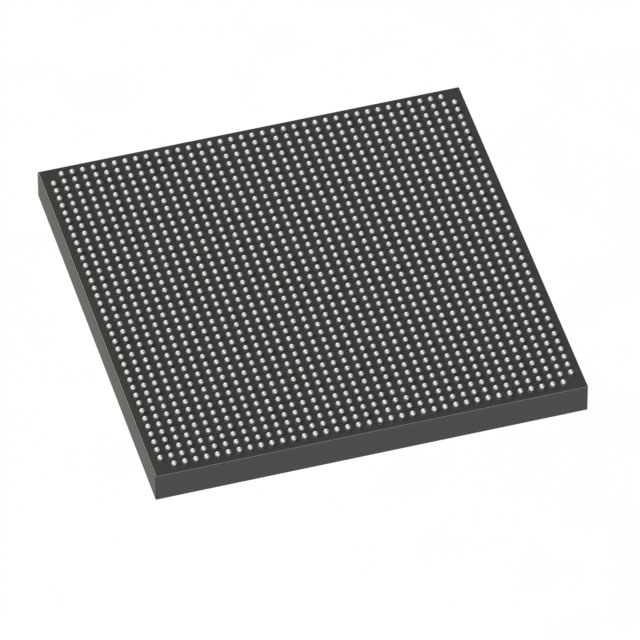
| Package / Case | 1932-BBGA, FCBGA | Number of I/O | 840 | Voltage | 870 mV - 930 mV | ||
| Mounting Method | Surface Mount | RoHS Compliance | RoHS non-compliant | REACH Compliance | REACH Unknown | ||
| Moisture Sensitivity Level | 3 (168 Hours) | Number of LABs/CLBs | 234720 | Number of Logic Elements/Cells | 622000 | ||
| Number of Gates | N/A | ECCN | 3A001A7A | HTS Code | 8542.39.0001 | ||
| Qualification | N/A | Total RAM Bits | 51200000 |
Overview of 5SGXEA7N1F45I2 – Stratix® V GX FPGA, 622,000 logic elements
The 5SGXEA7N1F45I2 is a Stratix V GX field-programmable gate array (FPGA) IC optimized for high-bandwidth, high-performance applications. It is built on the Stratix V family architecture and targets markets such as optical transport, packet processing, traffic management, wireline and military communications, and network test equipment.
This device pairs a high logic capacity with a large I/O count and substantial on-chip memory, delivered in a 1932-BBGA FCBGA package and specified for industrial temperature operation. The part is intended for designs that require dense programmable logic, extensive I/O, and on-chip memory resources within a 28-nm Stratix V device family feature set.
Key Features
- Logic Capacity — 622,000 logic elements suitable for complex programmable logic and system integration.
- Embedded Memory — Approximately 51.2 Mbits of on-chip RAM for buffering, packet processing, and large state machines.
- I/O Density — 840 user I/O pins to support broad interfacing and high-port-count system designs.
- Transceiver Family Capability — Stratix V GX devices in this family offer up to 66 integrated transceivers with 14.1-Gbps data rate capability for backplane and optical interfaces.
- Core and Fabric — Built on the Stratix V 28-nm family architecture with common features such as redesigned adaptive logic modules (ALMs), multi-track routing, and a comprehensive fabric clocking network.
- Embedded Hard IP — Includes the Stratix V Embedded HardCopy Block capability for hardening IP instantiation of PCIe Gen1/Gen2/Gen3 (family feature).
- Power Supply — Supported core voltage range of 870 mV to 930 mV as specified for the device.
- Package & Mounting — 1932-BBGA (FCBGA) package with surface-mount mounting; supplier package listed as 1932-FBGA, FC (45×45).
- Industrial Temperature Grade — Specified to operate from −40 °C to 100 °C for industrial applications.
- Manufacturing Process — Part of the Stratix V family manufactured on 28-nm process technology (family feature).
Typical Applications
- 40G/100G Optical Transport: Use integrated transceiver capability and high logic density to implement line modules, protocol processing, and transport aggregation functions.
- Packet Processing & Traffic Management: High logic element count and on-chip RAM enable complex packet buffering, classification, and high-throughput processing pipelines.
- Network Test Equipment: Dense I/O and programmable fabric support protocol emulation, traffic generation, and high-speed measurement functions.
- Wireline & Military Communications: Robust thermal range and high I/O count support rugged communications line cards and long-life deployments in demanding environments.
Unique Advantages
- High Logic Density: 622,000 logic elements provide the capacity for large, integrated system functions without external ASICs.
- Substantial On-Chip Memory: Approximately 51.2 Mbits of embedded RAM reduces external memory dependency for buffering and state storage.
- Broad I/O Connectivity: 840 I/Os enable flexible interfacing to high-port-count boards and multi-protocol systems.
- Family-Level Transceiver Support: Stratix V GX family transceivers support high-speed backplane and optical interfaces up to 14.1 Gbps, enabling high-bandwidth links.
- Industrial Temperature Rating: Specified −40 °C to 100 °C operation supports deployment in industrial and telecom environments.
- Proven Stratix V Architecture: Leverages the Stratix V family’s ALMs, M20K memory structure, and fabric clocking network for predictable implementation and integration.
Why Choose 5SGXEA7N1F45I2?
The 5SGXEA7N1F45I2 positions itself as a high-capacity, high-I/O FPGA option within the Stratix V GX family, offering a balance of dense logic, substantial embedded memory, and family-level high-speed transceiver capability. Its industrial temperature rating and surface-mount 1932-BBGA package make it suitable for communications and test equipment where thermal range and board-level integration matter.
Designers targeting packet processing, optical transport, and other bandwidth-centric applications will find the combination of logic elements, on-chip RAM, and I/O count useful for consolidating system functions and reducing external component count while leveraging the Stratix V family architecture and capabilities.
Request a quote or submit an inquiry to receive pricing and availability information for 5SGXEA7N1F45I2. Our team can assist with ordering details and lead-time estimates.


Date Founded: 1968
Headquarters: Santa Clara, California, USA
Employees: 130,000+
Revenue: $54.23 Billion
Certifications and Memberships: ISO9001:2015, ISO14001:2015, ISO17025:2017, ISO27001:2022, ISO45001:2018, ISO50001:2018


