
5SGXEA7N1F45I2N
| Part Description |
Stratix® V GX Field Programmable Gate Array (FPGA) IC 840 51200000 622000 1932-BBGA, FCBGA |
|---|---|
| Quantity | 1,027 Available (as of June 10, 2026) |
| Product Category | Field Programmable Gate Array (FPGA) |
|---|---|
| Manufacturer | Intel |
| Manufacturing Status | Obsolete |
| Manufacturer Standard Lead Time | Contact Us |
| Datasheet |
Specifications & Environmental
| Device Package | 1932-FBGA, FC (45x45) | Grade | Industrial | Operating Temperature | -40°C – 100°C | ||
|---|---|---|---|---|---|---|---|
| Package / Case | 1932-BBGA, FCBGA | Number of I/O | 840 | Voltage | 870 mV - 930 mV | ||
| Mounting Method | Surface Mount | RoHS Compliance | RoHS Compliant | REACH Compliance | REACH Unknown | ||
| Moisture Sensitivity Level | 3 (168 Hours) | Number of LABs/CLBs | 234720 | Number of Logic Elements/Cells | 622000 | ||
| Number of Gates | N/A | ECCN | 3A001A2C | HTS Code | 8542.39.0001 | ||
| Qualification | N/A | Total RAM Bits | 51200000 |
Overview of 5SGXEA7N1F45I2N – Stratix® V GX Field Programmable Gate Array (FPGA) IC
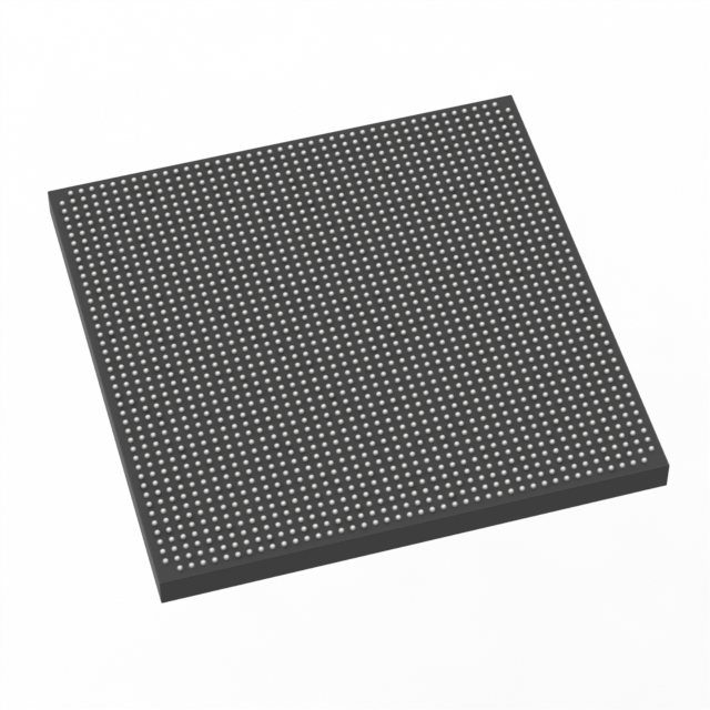
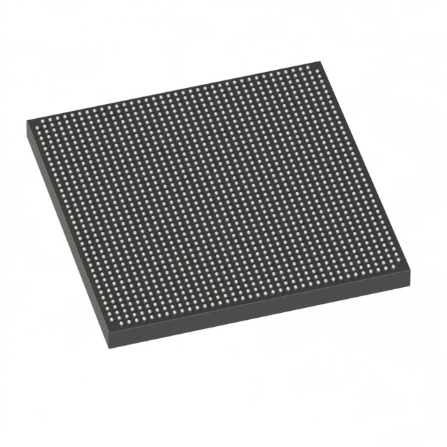
The 5SGXEA7N1F45I2N is a Stratix® V GX field-programmable gate array (FPGA) IC offered in an industrial temperature grade. It provides very large logic capacity, extensive on‑chip RAM, and a high I/O count in a 1932‑ball FCBGA package for high-density board designs.
Per the Stratix V device family datasheet, Stratix V GX devices are available across transceiver and core speed grades; the family includes transceiver speed grades documented up to 14.1 Gbps. This device is specified with key electrical and mechanical characteristics suitable for industrial-temperature FPGA applications.
Key Features
- Logic Capacity — 622,000 logic elements and 234,720 logic blocks provide very large programmable fabric for complex designs.
- Embedded Memory — Approximately 51.2 Mbits of on‑chip RAM for buffering, FIFOs, and local data storage.
- I/O Density — 840 user I/Os to support wide parallel interfaces and multiple peripherals.
- Package & Mounting — 1932‑BBGA (FCBGA) package; supplier device package noted as 1932‑FBGA, FC (45×45); surface‑mount device.
- Power Supply — Core voltage supply range specified at 870 mV to 930 mV.
- Temperature Grade — Industrial operating temperature range from −40 °C to 100 °C.
- Compliance — RoHS‑compliant.
- Family Transceiver Capability — Stratix V GX family transceiver speed grades are documented in the device datasheet (family entries include GX channel grades up to 14.1 Gbps and other supported grades).
Typical Applications
- Industrial control and automation — Industrial temperature rating and high I/O count enable deployment in control systems that require robust operation across −40 °C to 100 °C.
- High‑density custom logic — Large logic element count and substantial on‑chip RAM support complex, compute‑intensive FPGA designs and custom accelerators.
- High‑performance interface bridging — High I/O density and Stratix V GX family transceiver capabilities (per datasheet) suit designs that aggregate multiple high‑speed and parallel interfaces.
Unique Advantages
- Extensive programmable fabric: 622,000 logic elements and 234,720 logic blocks deliver the scale needed for large HDL designs and system integration on a single device.
- Significant on‑chip RAM: Approximately 51.2 Mbits of embedded memory reduces external memory dependency for buffering and on‑chip data handling.
- High I/O count: 840 I/Os simplify board‑level routing of multiple interfaces and peripherals without external expander logic.
- Industrial temperature rating: Specified operation from −40 °C to 100 °C addresses thermally demanding environments.
- Compact, high‑ball‑count package: 1932‑FBGA FCBGA package (45×45) concentrates resources in a compact footprint for high‑density PCB designs.
- Controlled core voltage range: 0.87–0.93 V core supply specification supports precise power sequencing and design planning.
Why Choose 5SGXEA7N1F45I2N?
The 5SGXEA7N1F45I2N positions itself as a high‑capacity Stratix V GX FPGA for industrial‑grade designs that demand large programmable logic, a substantial amount of embedded RAM, and a high I/O count in a dense FCBGA package. Its documented family transceiver capabilities and industrial temperature rating make it appropriate where both performance and extended temperature operation are required.
Engineers specifying this device will find a combination of scale and ruggedness suitable for complex system integration, high‑density logic consolidation, and designs that benefit from significant on‑chip memory and I/O resources.
Request a quote or submit an inquiry to obtain pricing and availability for the 5SGXEA7N1F45I2N.


Date Founded: 1968
Headquarters: Santa Clara, California, USA
Employees: 130,000+
Revenue: $54.23 Billion
Certifications and Memberships: ISO9001:2015, ISO14001:2015, ISO17025:2017, ISO27001:2022, ISO45001:2018, ISO50001:2018


