
5SGXEA7N2F40C1
| Part Description |
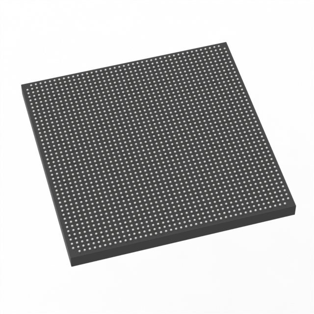
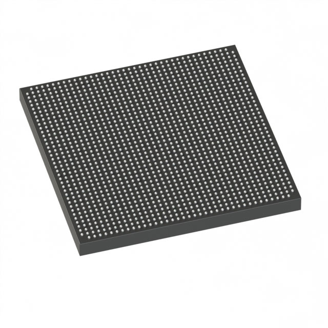
Stratix® V GX Field Programmable Gate Array (FPGA) IC 600 51200000 622000 1517-BBGA, FCBGA |
|---|---|
| Quantity | 1,334 Available (as of June 15, 2026) |

| Product Category | Field Programmable Gate Array (FPGA) |
|---|---|
| Manufacturer | Intel |
| Manufacturing Status | Obsolete |
| Manufacturer Standard Lead Time | Contact Us |
| Datasheet |
Specifications & Environmental
| Device Package | 1517-FBGA (40x40) | Grade | Commercial | Operating Temperature | 0°C – 85°C | ||
|---|---|---|---|---|---|---|---|
| Package / Case | 1517-BBGA, FCBGA | Number of I/O | 600 | Voltage | 870 mV - 930 mV | ||
| Mounting Method | Surface Mount | RoHS Compliance | RoHS Compliant | REACH Compliance | REACH Unknown | ||
| Moisture Sensitivity Level | 3 (168 Hours) | Number of LABs/CLBs | 234720 | Number of Logic Elements/Cells | 622000 | ||
| Number of Gates | N/A | ECCN | 3A001A2C | HTS Code | 8542.39.0001 | ||
| Qualification | N/A | Total RAM Bits | 51200000 |
Overview of 5SGXEA7N2F40C1 – Stratix® V GX FPGA; 622,000 logic elements, approximately 51.2 Mbits RAM, 600 I/Os
The 5SGXEA7N2F40C1 is a Stratix® V GX Field Programmable Gate Array (FPGA) IC from Intel designed for high-density, high-I/O digital designs. It delivers substantial programmable logic capacity and on-chip memory in a compact FCBGA package for commercial-grade applications.
With 622,000 logic elements, approximately 51.2 Mbits of embedded memory and 600 user I/Os, this device is targeted at systems that require large-scale logic integration, significant local buffering and broad I/O connectivity while operating within a commercial temperature range.
Key Features
- Core Capacity 622,000 logic elements for implementing large, complex digital designs and system-level integration.
- Embedded Memory Approximately 51.2 Mbits of on-chip RAM to support deep buffering, large FIFOs, and embedded data storage needs.
- I/O Integration 600 I/Os to accommodate wide external interfaces, parallel buses, and diverse peripheral connections.
- Power Supply Core voltage supply range of 870 mV to 930 mV, enabling designs that require defined low-voltage core operation.
- Package & Mounting 1517-BBGA (FCBGA) package; supplier device package listed as 1517-FBGA (40×40). Device is surface-mount for standard PCB assembly flows.
- Commercial Grade & Temperature Commercial temperature grade with an operating range of 0 °C to 85 °C for mainstream electronics products.
- Standards Compliance RoHS compliant for environmental and regulatory alignment in commercial product builds.
- Stratix V GX Family Transceiver Capabilities (series) Per the Stratix V device documentation, GX family transceiver speed grades are provided for high-speed serial channels in the series datasheet.
Typical Applications
- High-density digital processing Large programmable logic capacity and on-chip RAM make the device suitable for complex signal processing and algorithm acceleration inside a single FPGA.
- Networking and telecommunications High I/O count and Stratix V GX family transceiver capabilities support dense interface requirements in networking line cards and telecom equipment.
- Data center and compute acceleration Significant logic and memory resources enable offload and acceleration functions where on-chip integration reduces board-level complexity.
- High-speed serial communications Stratix V GX series transceiver grades (as listed in the family datasheet) provide options for high-throughput serial links as part of system designs.
Unique Advantages
- Massive programmable capacity: 622,000 logic elements combined with ~51.2 Mbits of embedded memory reduces reliance on external logic and memory components.
- Broad I/O integration: 600 I/Os allow integration of multiple parallel and serial interfaces without extensive external glue logic.
- Compact BBGA package: 1517-BBGA (1517-FBGA 40×40) surface-mount footprint balances density and manufacturability for commercial products.
- Commercial-grade operating range: Rated for 0 °C to 85 °C operation and RoHS compliance for mainstream product deployment.
- Stratix V GX family documentation: Backed by the family datasheet and technical documentation for device-level electrical and switching characteristics.
Why Choose 5SGXEA7N2F40C1?
The 5SGXEA7N2F40C1 positions itself as a high-capacity, high-I/O Stratix V GX FPGA for commercial applications that require extensive programmable logic, sizable on-chip memory, and many external interfaces. Its 1517-BBGA surface-mount package and defined core supply range make it suitable for mainstream electronic product designs that prioritize integration and board-level density.
Engineers and procurement teams seeking a large, commercial-grade Stratix V GX device will find this part aligns with projects that demand significant local resources and clear family-level device documentation from Intel.
Request a quote or submit a purchase inquiry to obtain pricing and availability for the 5SGXEA7N2F40C1.


Date Founded: 1968
Headquarters: Santa Clara, California, USA
Employees: 130,000+
Revenue: $54.23 Billion
Certifications and Memberships: ISO9001:2015, ISO14001:2015, ISO17025:2017, ISO27001:2022, ISO45001:2018, ISO50001:2018


