
5SGXEB5R2F43C2G
| Part Description |
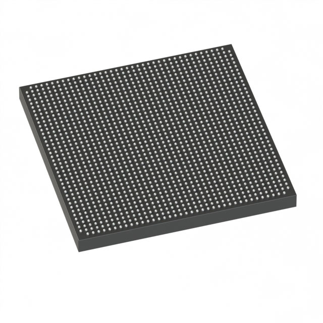
Stratix® V GX Field Programmable Gate Array (FPGA) IC 600 41984000 490000 1760-BBGA, FCBGA |
|---|---|
| Quantity | 841 Available (as of June 14, 2026) |

| Product Category | Field Programmable Gate Array (FPGA) |
|---|---|
| Manufacturer | Intel |
| Manufacturing Status | Active |
| Manufacturer Standard Lead Time | 26 Weeks |
| Datasheet |
Specifications & Environmental
| Device Package | 1760-FCBGA (42.5x42.5) | Grade | Commercial | Operating Temperature | 0°C – 85°C | ||
|---|---|---|---|---|---|---|---|
| Package / Case | 1760-BBGA, FCBGA | Number of I/O | 600 | Voltage | 870 mV - 930 mV | ||
| Mounting Method | Surface Mount | RoHS Compliance | RoHS Compliant | REACH Compliance | REACH Unaffected | ||
| Moisture Sensitivity Level | 3 (168 Hours) | Number of LABs/CLBs | 185000 | Number of Logic Elements/Cells | 490000 | ||
| Number of Gates | N/A | ECCN | N/A | HTS Code | N/A | ||
| Qualification | N/A | Total RAM Bits | 41984000 |
Overview of 5SGXEB5R2F43C2G – Stratix V GX FPGA, 1760‑FCBGA
The 5SGXEB5R2F43C2G is a Stratix® V GX field‑programmable gate array (FPGA) in a 1760‑ball FCBGA package intended for commercial applications. It combines a high density of logic elements, substantial on‑chip memory, and extensive I/O to support complex, high‑integration digital designs.
Targeted at designs that require large programmable logic capacity and dense connectivity, this device is suited for advanced data processing, communications, and compute acceleration in commercial temperature environments.
Key Features
- High Logic Capacity Approximately 490,000 logic elements to implement large, complex logic designs on a single device.
- Embedded Memory Approximately 42 Mbits of on‑chip RAM for buffer, cache, and real‑time data storage needs.
- Extensive I/O 600 I/O pins provide broad external connectivity for interfaces, parallel buses, and high‑density routing.
- Power/Core Supply Core operating voltage range of 870 mV to 930 mV to match target power‑domain designs.
- Commercial Temperature Grade Rated for 0 °C to 85 °C operation for commercial‑grade system deployment.
- Package & Mounting 1760‑FCBGA (42.5 × 42.5 mm) surface‑mount package for compact, high‑pin‑count PCB designs.
- RoHS Compliant Conforms to RoHS requirements for lead‑free manufacturing compliance.
Typical Applications
- High‑density Data Processing On‑chip logic and memory enable implementation of custom data pipelines, packet processing, and hardware acceleration functions.
- Communications Systems Large logic capacity and abundant I/O support protocol handling, framing, and interface aggregation in commercial networking equipment.
- Compute Acceleration Use as a reconfigurable accelerator for algorithm offload where substantial programmable logic and local RAM reduce external memory dependency.
- Test & Measurement Flexible I/O and significant internal resources make the device suitable for instrument control, real‑time processing, and custom measurement logic.
Unique Advantages
- Large single‑chip integration: Consolidates complex logic and memory on one FPGA, reducing board complexity and BOM count.
- High I/O density: 600 I/Os enable multiple interfaces and parallel connections without external multiplexing hardware.
- Commercial‑grade design: Specified 0 °C to 85 °C operation and RoHS compliance for mainstream product deployments.
- Compact high‑pin package: 1760‑FCBGA (42.5 × 42.5 mm) balances pin count and board area for dense PCB layouts.
- Controlled core supply range: Defined 870 mV–930 mV voltage range supports predictable power design and regulation requirements.
Why Choose 5SGXEB5R2F43C2G?
The 5SGXEB5R2F43C2G delivers a combination of high logic density, substantial embedded RAM, and extensive I/O in a commercial‑grade Stratix V GX FPGA package. It is well suited for designers who need to implement large, integrative digital systems on a single device while maintaining compact PCB footprint and predictable power characteristics.
Choose this device when your design demands significant programmable logic and on‑chip memory with dense external connectivity in a RoHS‑compliant, surface‑mount FCBGA package.
Request a quote or submit your procurement inquiry to obtain pricing and availability for the 5SGXEB5R2F43C2G.


Date Founded: 1968
Headquarters: Santa Clara, California, USA
Employees: 130,000+
Revenue: $54.23 Billion
Certifications and Memberships: ISO9001:2015, ISO14001:2015, ISO17025:2017, ISO27001:2022, ISO45001:2018, ISO50001:2018


