
5SGXEB5R2F43C2
| Part Description |
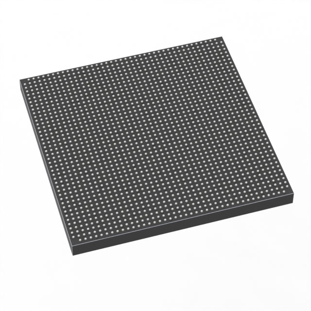
Stratix® V GX Field Programmable Gate Array (FPGA) IC 600 41984000 490000 1760-BBGA, FCBGA |
|---|---|
| Quantity | 279 Available (as of June 10, 2026) |

| Product Category | Field Programmable Gate Array (FPGA) |
|---|---|
| Manufacturer | Intel |
| Manufacturing Status | Obsolete |
| Manufacturer Standard Lead Time | Contact Us |
| Datasheet |
Specifications & Environmental
| Device Package | 1760-FCBGA (42.5x42.5) | Grade | Commercial | Operating Temperature | 0°C – 85°C | ||
|---|---|---|---|---|---|---|---|
| Package / Case | 1760-BBGA, FCBGA | Number of I/O | 600 | Voltage | 870 mV - 930 mV | ||
| Mounting Method | Surface Mount | RoHS Compliance | RoHS Compliant | REACH Compliance | REACH Unknown | ||
| Moisture Sensitivity Level | 3 (168 Hours) | Number of LABs/CLBs | 185000 | Number of Logic Elements/Cells | 490000 | ||
| Number of Gates | N/A | ECCN | OBSOLETE | HTS Code | N/A | ||
| Qualification | N/A | Total RAM Bits | 41984000 |
Overview of 5SGXEB5R2F43C2 – Stratix® V GX FPGA, 1760-FCBGA (Commercial)
The 5SGXEB5R2F43C2 is a Stratix® V GX family field programmable gate array (FPGA) in a 1760-ball FCBGA package designed for high-density, high-connectivity designs. It combines a large logic fabric with substantial on-chip memory and a high I/O count to address complex digital signal processing, prototyping, and system integration tasks.
With 490,000 logic elements, approximately 42 Mbits of embedded memory, and support for Stratix V GX device transceiver options (see device documentation for speed grades), this device targets applications that require significant programmable logic, dense external interfacing, and low-voltage core operation.
Key Features
- Core / Logic 490,000 logic elements provide extensive programmable logic resources for large designs and complex algorithm implementation.
- Embedded Memory Approximately 42 Mbits of on-chip RAM (41,984,000 bits) for large buffering, lookup tables, and state storage without external memory.
- I/O & Connectivity 600 general-purpose I/O pins enable dense peripheral and board-level interfacing for multi-channel systems and high-pin-count designs.
- Power Core voltage supply range of 870 mV to 930 mV to match low-voltage system power domains.
- Package & Mounting 1760-ball FCBGA package (1760-FCBGA, 42.5 × 42.5 mm) in a surface-mount form factor for high-density board integration and thermal management.
- Temperature & Grade Commercial grade operation with an ambient range of 0 °C to 85 °C for standard commercial applications.
- Regulatory RoHS compliant.
Typical Applications
- High‑performance Prototyping Large logic capacity and substantial on-chip RAM make this FPGA suitable for complex prototype systems and hardware emulation.
- Communications & Networking High I/O count supports multi‑lane interfaces and dense front‑end connectivity for network processing and protocol handling; Stratix V GX family transceiver options support high-speed link configurations per device documentation.
- Signal Processing Large logic and memory resources support DSP pipelines, video/graphics preprocessing, and data aggregation tasks.
- System Integration The 1760-FCBGA package and surface-mount mounting simplify integration into compact, high-density system boards.
Unique Advantages
- High Logic Density: 490,000 logic elements allow consolidation of large functions on a single device, reducing board-level complexity.
- Substantial Embedded Memory: Approximately 42 Mbits of on-chip RAM minimizes dependence on external memory for buffering and state retention.
- Extensive I/O Resources: 600 I/Os enable direct connection to multiple peripherals, interfaces, and mezzanine cards without complex routing compromises.
- Low‑Voltage Core Operation: 870–930 mV supply range aligns with low-voltage power architectures to support power-optimized system designs.
- Commercial Temperature Rating: Designed for standard commercial environments (0 °C to 85 °C), suitable for a wide range of consumer and enterprise applications.
- RoHS Compliant: Meets common environmental regulatory requirements for easier product acceptance and manufacturing.
Why Choose 5SGXEB5R2F43C2?
The 5SGXEB5R2F43C2 brings together a high-density Stratix V GX architecture, very large on-chip memory, and a 600-pin I/O envelope in a single 1760-FCBGA package. It is suited to designers who need to implement complex digital systems with significant internal storage and dense external connectivity while operating within commercial temperature ranges and low-voltage power domains.
For teams building high-performance prototypes, communications infrastructure, or advanced signal-processing modules, this device offers a scalable, integrated platform with the documented capabilities of the Stratix V GX family and the capacity to consolidate multiple functions onto a single FPGA to simplify BOM and board layout.
Request a quote or submit an RFQ to receive pricing, availability, and ordering information for the 5SGXEB5R2F43C2.


Date Founded: 1968
Headquarters: Santa Clara, California, USA
Employees: 130,000+
Revenue: $54.23 Billion
Certifications and Memberships: ISO9001:2015, ISO14001:2015, ISO17025:2017, ISO27001:2022, ISO45001:2018, ISO50001:2018


