
5SGXEB6R2F40C3
| Part Description |
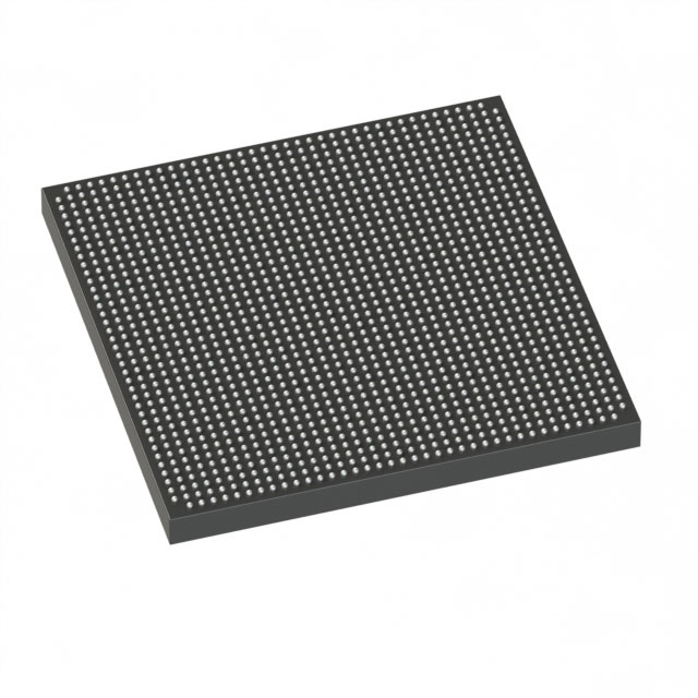
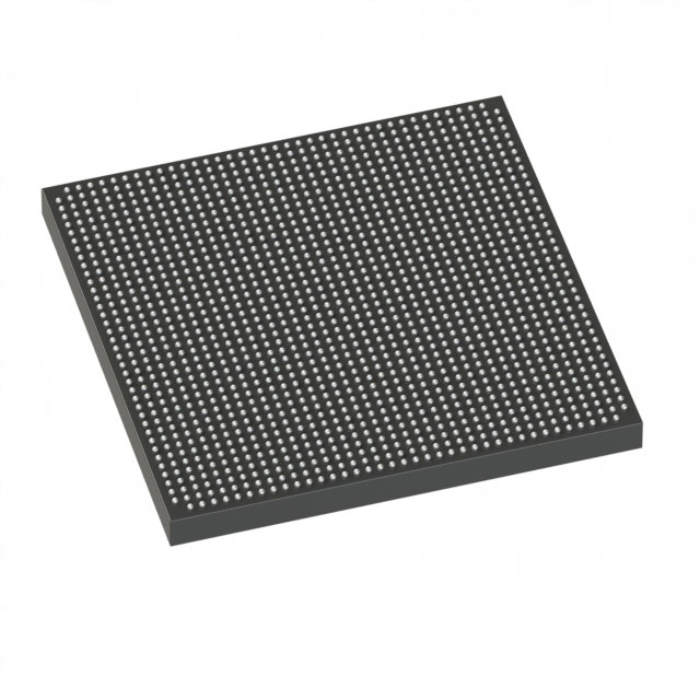
Stratix® V GX Field Programmable Gate Array (FPGA) IC 432 53248000 597000 1517-FBGA (40x40) |
|---|---|
| Quantity | 771 Available (as of October 7, 2026) |
| Product Category | Field Programmable Gate Array (FPGA) |
|---|---|
| Manufacturer | Intel |
| Manufacturing Status | Obsolete |
| Manufacturer Standard Lead Time | Contact Us |
| Datasheet |
Specifications & Environmental
| Device Package | 1517-FBGA (40x40) | Grade | Commercial | Operating Temperature | 0°C – 85°C | ||
|---|---|---|---|---|---|---|---|
| Package / Case | 1517-FBGA (40x40) | Number of I/O | 432 | Voltage | 820 mV - 880 mV | ||
| Mounting Method | Surface Mount | RoHS Compliance | RoHS Compliant | REACH Compliance | REACH Unknown | ||
| Moisture Sensitivity Level | 3 (168 Hours) | Number of LABs/CLBs | 225400 | Number of Logic Elements/Cells | 597000 | ||
| Number of Gates | N/A | ECCN | 3A001A2C | HTS Code | 8542.39.0001 | ||
| Qualification | N/A | Total RAM Bits | 53248000 |
Overview of 5SGXEB6R2F40C3 – Stratix® V GX FPGA, 597,000 logic elements, 1517‑FBGA (40×40)
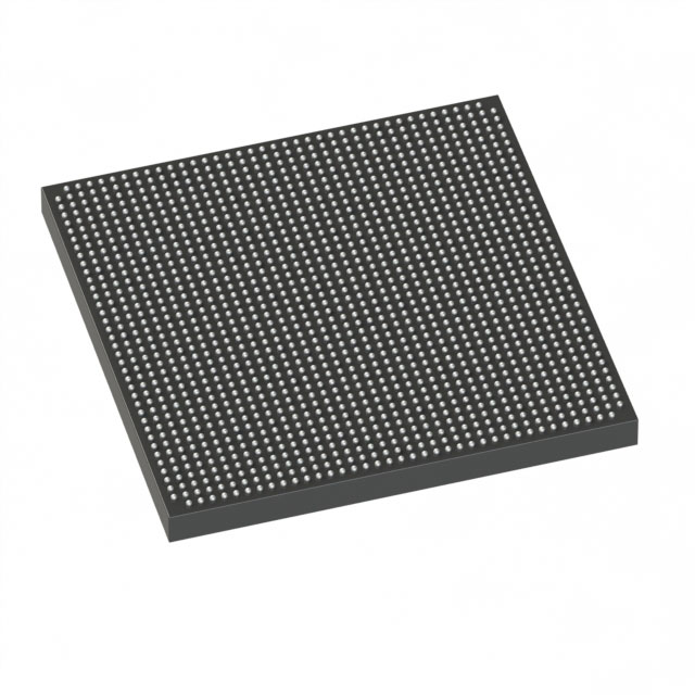
The 5SGXEB6R2F40C3 is a Stratix® V GX Field Programmable Gate Array (FPGA) IC designed for complex digital designs requiring large logic capacity and substantial on‑chip memory. It implements the Stratix V GX architecture and is provided in a 1517‑FBGA (40×40) surface‑mount package for compact system integration.
With hundreds of thousands of logic elements, tens of megabits of embedded RAM, and a broad I/O count, this device targets applications that demand dense programmable logic, embedded memory, and flexible I/O in a commercial‑grade temperature range.
Key Features
- Core logic Approximately 597,000 logic elements to support large, complex FPGA designs and high gate-count implementations.
- Embedded memory Approximately 53.25 Mbits of on‑chip RAM for buffering, state storage, and memory‑intensive functions.
- I/O and package 432 user I/O pins in a 1517‑FBGA (40×40) surface‑mount package for dense connectivity and compact board footprint.
- Power supply Core supply nominal range specified at 0.820 V to 0.880 V to guide power‑delivery and thermal budgeting.
- Temperature and grade Commercial grade device rated for 0 °C to 85 °C operating temperature.
- Regulatory RoHS compliant.
- Family characteristics Part of the Stratix V GX family; refer to the Stratix V device datasheet for details on device-level electrical and transceiver characteristics.
Typical Applications
- High‑capacity digital systems Large logic capacity and embedded RAM make this device suitable for complex compute and control fabrics.
- Video and signal processing On‑chip memory and abundant logic resources support buffering, pipelined processing, and algorithm acceleration.
- Communications infrastructure High I/O count and Stratix V GX family transceiver capabilities (see device datasheet) enable implementation of custom interface logic and protocol processing.
Unique Advantages
- High logic density: ~597,000 logic elements provide the capacity needed for large, integrated FPGA designs without immediate migration to multiple devices.
- Substantial embedded RAM: Approximately 53.25 Mbits of on‑chip memory reduces external memory dependence for many buffering and state‑storage needs.
- Generous I/O in a compact package: 432 I/O pins in a 1517‑FBGA (40×40) surface‑mount package balance connectivity and board space efficiency.
- Defined power envelope: Core voltage range of 0.820 V–0.880 V enables predictable power‑delivery design and thermal planning.
- Commercial temperature support: Rated for 0 °C–85 °C operations for standard commercial deployments.
- RoHS compliant: Environmentally compliant for regions and customers that require RoHS conformity.
Why Choose 5SGXEB6R2F40C3?
The 5SGXEB6R2F40C3 delivers a combination of large logic capacity, meaningful on‑chip memory, and a high I/O count in a compact 1517‑FBGA package. Its Stratix V GX pedigree and the electrical characteristics documented in the device datasheet make it a suitable choice for designers who need a dense, programmable logic solution within a commercial temperature envelope.
This part is appropriate for design teams building complex digital signal processing, communications, or high‑density control systems that require significant on‑chip resources, predictable power rails, and compact package integration.
Request a quote or contact sales to discuss availability, volume pricing, and integration support for the 5SGXEB6R2F40C3.





















Date Founded: 1968
Headquarters: Santa Clara, California, USA
Employees: 130,000+
Revenue: $54.23 Billion
Certifications and Memberships: ISO9001:2015, ISO14001:2015, ISO17025:2017, ISO27001:2022, ISO45001:2018, ISO50001:2018


