
5SGXEB6R2F40I2LN
| Part Description |
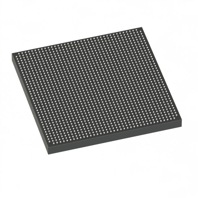
Stratix® V GX Field Programmable Gate Array (FPGA) IC 432 53248000 597000 1517-FBGA (40x40) |
|---|---|
| Quantity | 1,076 Available (as of June 14, 2026) |

| Product Category | Field Programmable Gate Array (FPGA) |
|---|---|
| Manufacturer | Intel |
| Manufacturing Status | Obsolete |
| Manufacturer Standard Lead Time | Contact Us |
| Datasheet |
Specifications & Environmental
| Device Package | 1517-FBGA (40x40) | Grade | Industrial | Operating Temperature | -40°C – 100°C | ||
|---|---|---|---|---|---|---|---|
| Package / Case | 1517-FBGA (40x40) | Number of I/O | 432 | Voltage | 820 mV - 880 mV | ||
| Mounting Method | Surface Mount | RoHS Compliance | RoHS Compliant | REACH Compliance | REACH Unknown | ||
| Moisture Sensitivity Level | 3 (168 Hours) | Number of LABs/CLBs | 225400 | Number of Logic Elements/Cells | 597000 | ||
| Number of Gates | N/A | ECCN | 3A001A2C | HTS Code | 8542.39.0001 | ||
| Qualification | N/A | Total RAM Bits | 53248000 |
Overview of 5SGXEB6R2F40I2LN – Stratix® V GX FPGA, 597,000 logic elements, approximately 53.248 Mbits RAM, 432 I/Os, 1517-FBGA (40×40)
The 5SGXEB6R2F40I2LN is an Intel Stratix® V GX Field Programmable Gate Array (FPGA) in a 1517-FBGA (40×40) surface-mount package. It delivers high logic capacity and on‑chip memory in an industrial-grade device designed for demanding embedded designs.
With 597,000 logic elements, approximately 53.248 Mbits of embedded RAM, and 432 available I/Os, this device targets complex, I/O- and memory-intensive systems. The device is specified for industrial operation and supports a core supply range of 820 mV to 880 mV and an operating temperature range of −40 °C to 100 °C.
Key Features
- Core Logic 597,000 logic elements to implement large-scale programmable logic, state machines, and custom datapaths.
- Embedded Memory Approximately 53.248 Mbits of on-chip RAM for buffering, packet storage, and data processing without external memory dependence.
- I/O Density 432 I/Os to support extensive peripheral, sensor, and subsystem interfacing on a single FPGA.
- Power and Voltage Core supply range of 820 mV to 880 mV to match system power-rail design and regulator selection requirements.
- Package & Mounting 1517-FBGA (40×40) surface-mount package for high-density PCB integration and robust soldered attachment.
- Temperature & Grade Industrial grade device specified for operation from −40 °C to 100 °C, suitable for temperature-challenging environments.
- Series Transceiver Capability (Series-level) The Stratix V GX family includes high-speed transceiver options (series documentation cites GX channel capability up to 14.1 Gbps), enabling high-bandwidth serial links where required.
- Compliance RoHS compliant, supporting regulatory and manufacturing requirements for lead-free assembly.
Typical Applications
- I/O‑intensive systems — Use the device’s 432 I/Os for dense sensor arrays, board-level interfacing, or complex digital I/O routing.
- Memory‑heavy processing — On‑chip RAM capacity supports packet buffering, local data caching, and intermediate storage for streaming algorithms.
- Industrial control and instrumentation — Industrial-grade temperature range and robust packaging suit factory automation, test equipment, and control systems.
- High‑speed serial link subsystems — Leverage Stratix V GX family transceiver capabilities for high-bandwidth serial communications and link aggregation designs.
Unique Advantages
- High logic density: 597,000 logic elements enable consolidation of large FPGA designs onto a single device, reducing board count.
- Substantial embedded memory: Approximately 53.248 Mbits of on-chip RAM helps minimize external memory requirements and simplifies PCB layout.
- Extensive I/O: 432 I/Os provide flexible connectivity for complex system integration and peripheral interfacing.
- Industrial readiness: Specified −40 °C to 100 °C operating range and industrial grade designation support deployment in harsh environments.
- Compact, high-density package: 1517-FBGA (40×40) surface-mount package enables dense PCB integration while maintaining signal routing options.
- Regulatory compliance: RoHS compliance supports lead-free assembly and environmental manufacturing requirements.
Why Choose 5SGXEB6R2F40I2LN?
The 5SGXEB6R2F40I2LN positions itself as a high-capacity FPGA option within the Stratix V GX family, combining large logic resources, significant on‑chip memory, and a high I/O count in an industrial-grade package. These characteristics make it suitable for developers tackling complex, memory- and I/O-intensive applications that require reliable operation across extended temperature ranges.
Backed by Intel’s Stratix V device documentation and series-level transceiver capabilities, this part is appropriate for engineering teams seeking a scalable, high-density programmable logic device that integrates into mature design flows. Its combination of density, memory, and industrial specification supports long-term deployments and iterative design scaling.
Request a quote or submit an inquiry to obtain pricing, lead time, and availability for the 5SGXEB6R2F40I2LN.


Date Founded: 1968
Headquarters: Santa Clara, California, USA
Employees: 130,000+
Revenue: $54.23 Billion
Certifications and Memberships: ISO9001:2015, ISO14001:2015, ISO17025:2017, ISO27001:2022, ISO45001:2018, ISO50001:2018


