
5SGXEB6R3F40C4G
| Part Description |
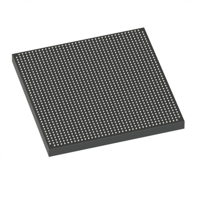
Stratix® V GX Field Programmable Gate Array (FPGA) IC 432 53248000 597000 1517-FBGA (40x40) |
|---|---|
| Quantity | 349 Available (as of June 15, 2026) |

| Product Category | Field Programmable Gate Array (FPGA) |
|---|---|
| Manufacturer | Intel |
| Manufacturing Status | Active |
| Manufacturer Standard Lead Time | 26 Weeks |
| Datasheet |
Specifications & Environmental
| Device Package | 1517-FBGA (40x40) | Grade | Commercial | Operating Temperature | 0°C – 85°C | ||
|---|---|---|---|---|---|---|---|
| Package / Case | 1517-FBGA (40x40) | Number of I/O | 432 | Voltage | 820 mV - 880 mV | ||
| Mounting Method | Surface Mount | RoHS Compliance | RoHS Compliant | REACH Compliance | REACH Unaffected | ||
| Moisture Sensitivity Level | 3 (168 Hours) | Number of LABs/CLBs | 225400 | Number of Logic Elements/Cells | 597000 | ||
| Number of Gates | N/A | ECCN | N/A | HTS Code | N/A | ||
| Qualification | N/A | Total RAM Bits | 53248000 |
Overview of 5SGXEB6R3F40C4G – Stratix® V GX Field Programmable Gate Array (FPGA) IC 432 53248000 597000 1517-FBGA (40x40)
The 5SGXEB6R3F40C4G is a Stratix V GX field-programmable gate array (FPGA) from Intel, offered in a 1517-FBGA (40x40) surface-mount package. It provides a high-capacity programmable fabric combined with extensive I/O and embedded memory for demanding logic and I/O timing applications.
Designed for commercial-temperature operation, this device targets high-density programmable logic and high-speed I/O use cases where on-chip memory, a large population of logic elements, and documented electrical and switching characteristics are required.
Key Features
- Core density Approximately 597,000 logic elements to implement large, complex designs.
- Embedded memory Approximately 53.2 Mbits of on-chip RAM for buffering, FIFOs, and local storage.
- I/O 432 general-purpose I/O pins to support wide parallel interfaces and multiple peripherals.
- Package & mounting 1517-FBGA (40x40) package in a surface-mount form factor for board-level integration.
- Power supply Core voltage supply range: 820 mV to 880 mV, enabling defined operating conditions for the device core.
- Operating range Commercial temperature grade with an operating temperature range of 0 °C to 85 °C.
- Programmable I/O timing Datasheet documents I/O timing features, including programmable I/O element (IOE) delay and programmable output buffer delay for fine-grained timing control.
- Transceiver-capable series Stratix V GX devices are described in the series datasheet with transceiver speed grade options and switching characteristic information.
- Compliance RoHS-compliant.
Typical Applications
- High-speed communications Leverage the Stratix V GX family’s transceiver-capable architecture and documented switching characteristics for designs requiring robust I/O timing and high-speed links.
- Network and data processing High logic density and substantial on-chip memory make the device suitable for packet processing, bridging, and protocol handling tasks.
- Advanced signal processing Large logic capacity and embedded RAM enable implementation of complex signal processing pipelines and on-chip buffering.
Unique Advantages
- High integration density: Approximately 597,000 logic elements reduce the need for multiple devices in complex designs.
- Significant on-chip memory: Approximately 53.2 Mbits of embedded RAM supports large buffers, lookup tables, and local storage without external memory.
- Extensive I/O count: 432 I/O pins allow broad connectivity for parallel interfaces and multiple peripherals.
- Documented I/O timing controls: Programmable IOE delay and output buffer delay options documented in the Stratix V device datasheet help with timing closure and signal integrity.
- Compact board footprint: 1517-FBGA (40x40) package in a surface-mount form factor supports dense board designs.
- Commercial-grade robustness: Rated for 0 °C to 85 °C operation and RoHS-compliant for standard commercial deployments.
Why Choose 5SGXEB6R3F40C4G?
The 5SGXEB6R3F40C4G delivers a combination of high logic capacity, substantial embedded memory, and abundant I/O in a compact FBGA package, making it well suited for commercial applications that require dense programmable logic and careful I/O timing. Its documented electrical and switching characteristics in the Stratix V device datasheet support design verification and system-level integration.
Backed by Intel’s Stratix V device documentation, this FPGA is positioned for designers who need scalable logic density, on-chip RAM for buffering and processing, and a high I/O count in a surface-mount footprint.
Request a quote or submit your specifications to receive pricing and availability for the 5SGXEB6R3F40C4G.


Date Founded: 1968
Headquarters: Santa Clara, California, USA
Employees: 130,000+
Revenue: $54.23 Billion
Certifications and Memberships: ISO9001:2015, ISO14001:2015, ISO17025:2017, ISO27001:2022, ISO45001:2018, ISO50001:2018


