
5SGXEB6R3F40I3LG
| Part Description |
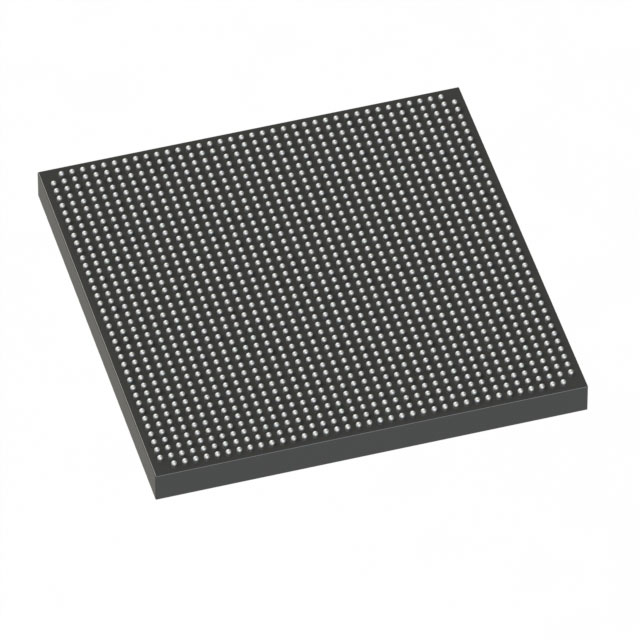
Stratix® V GX Field Programmable Gate Array (FPGA) IC 432 53248000 597000 1517-FBGA (40x40) |
|---|---|
| Quantity | 481 Available (as of June 15, 2026) |

| Product Category | Field Programmable Gate Array (FPGA) |
|---|---|
| Manufacturer | Intel |
| Manufacturing Status | Active |
| Manufacturer Standard Lead Time | 26 Weeks |
| Datasheet |
Specifications & Environmental
| Device Package | 1517-FBGA (40x40) | Grade | Industrial | Operating Temperature | -40°C – 100°C | ||
|---|---|---|---|---|---|---|---|
| Package / Case | 1517-FBGA (40x40) | Number of I/O | 432 | Voltage | 820 mV - 880 mV | ||
| Mounting Method | Surface Mount | RoHS Compliance | RoHS Compliant | REACH Compliance | REACH Unaffected | ||
| Moisture Sensitivity Level | 3 (168 Hours) | Number of LABs/CLBs | 225400 | Number of Logic Elements/Cells | 597000 | ||
| Number of Gates | N/A | ECCN | N/A | HTS Code | N/A | ||
| Qualification | N/A | Total RAM Bits | 53248000 |
Overview of 5SGXEB6R3F40I3LG – Stratix V GX FPGA, 1517-FBGA (40×40)
The 5SGXEB6R3F40I3LG is an Intel Stratix® V GX field-programmable gate array supplied in a 1517-FBGA (40×40) package. This industrial-grade FPGA integrates high logic density, substantial embedded memory, and abundant I/O in a surface-mount BGA package for demanding embedded and system-level designs.
With approximately 597,000 logic elements, around 53.25 Mbits of on-chip RAM, and 432 I/Os, the device is suited to applications that require high integration, significant on-chip storage, and extensive I/O connectivity. Series-level documentation for Stratix V GX devices also describes multi-gigabit transceiver speed grades used across the family.
Key Features
- Core & Logic density Approximately 597,000 logic elements enable complex digital designs and high-functional integration on a single device.
- Embedded memory Approximately 53.25 Mbits of on-chip RAM for buffering, lookup tables, and large on-chip data structures.
- I/O capacity 432 user I/Os provide broad connectivity for peripherals, parallel buses, and external interfaces.
- Transceiver capability (series-level) Stratix V GX series documentation specifies multiple transceiver speed grades (up to 14.1 Gbps in the series), enabling high-speed serial links where supported by the device family.
- Power Voltage supply range specified at 0.820–0.880 V for core operation to support targeted power domains and system-level power planning.
- Package & mounting 1517-FBGA (40×40) supplier device package with surface-mount mounting type for compact board-level implementation.
- Industrial operating range Rated for −40 °C to 100 °C operation, suitable for industrial-temperature applications.
- Regulatory status RoHS compliant.
Typical Applications
- High-density digital systems Implement complex state machines, custom accelerators, and dense logic partitions using the device’s large logic element count.
- On-chip buffering and memory-centric designs Use approximately 53.25 Mbits of embedded RAM for packet buffering, FIFOs, and large LUT-based structures without external memory.
- Multi-I/O interface hubs Leverage 432 I/Os to aggregate sensors, buses, and peripheral interfaces on a single FPGA for system consolidation.
- High-speed serial connectivity (where supported) Within the Stratix V GX family transceiver speed grades, support for multi-gigabit serial links enables high-throughput channel designs.
Unique Advantages
- High logic capacity: Enables consolidation of complex functions and reduces the need for multiple devices in dense designs.
- Substantial embedded memory: Approximately 53.25 Mbits of on-chip RAM reduces dependency on external memory components and simplifies board design.
- Extensive I/O count: 432 I/Os provide flexibility to connect numerous peripherals or wide parallel interfaces directly to the FPGA.
- Industrial temperature rating: Specified −40 °C to 100 °C operation supports deployment in industrial environments.
- Compact BGA package: 1517-FBGA (40×40) surface-mount packaging balances high integration with board-space efficiency.
- RoHS compliance: Aligns with common regulatory and environmental requirements for electronic assemblies.
Why Choose 5SGXEB6R3F40I3LG?
The 5SGXEB6R3F40I3LG delivers a combination of high logic density, large on-chip RAM, and abundant I/O in an industrial-grade Stratix V GX FPGA footprint. It is well suited for engineers needing a single-chip solution for complex digital processing, large buffering needs, and extensive peripheral interfacing within a compact BGA package.
Choosing this Stratix V GX part provides scalability and design headroom for demanding embedded and system-level applications, while the industrial temperature rating and RoHS compliance support reliable deployment in regulated and harsh environments.
Request a quote or submit an inquiry to receive pricing, availability, and lead-time information for the 5SGXEB6R3F40I3LG. Technical datasheet details are available for review to support integration and design planning.


Date Founded: 1968
Headquarters: Santa Clara, California, USA
Employees: 130,000+
Revenue: $54.23 Billion
Certifications and Memberships: ISO9001:2015, ISO14001:2015, ISO17025:2017, ISO27001:2022, ISO45001:2018, ISO50001:2018


