
5SGXEB6R3F43C2
| Part Description |
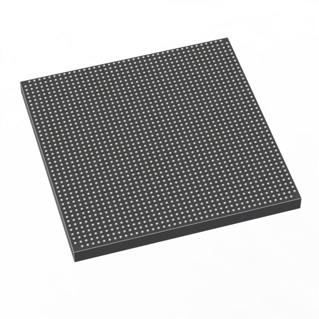
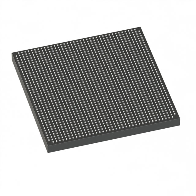
Stratix® V GX Field Programmable Gate Array (FPGA) IC 600 53248000 597000 1760-BBGA, FCBGA |
|---|---|
| Quantity | 181 Available (as of June 14, 2026) |

| Product Category | Field Programmable Gate Array (FPGA) |
|---|---|
| Manufacturer | Intel |
| Manufacturing Status | Obsolete |
| Manufacturer Standard Lead Time | Contact Us |
| Datasheet |
Specifications & Environmental
| Device Package | 1760-FCBGA (42.5x42.5) | Grade | Commercial | Operating Temperature | 0°C – 85°C | ||
|---|---|---|---|---|---|---|---|
| Package / Case | 1760-BBGA, FCBGA | Number of I/O | 600 | Voltage | 870 mV - 930 mV | ||
| Mounting Method | Surface Mount | RoHS Compliance | RoHS Compliant | REACH Compliance | REACH Unknown | ||
| Moisture Sensitivity Level | 3 (168 Hours) | Number of LABs/CLBs | 225400 | Number of Logic Elements/Cells | 597000 | ||
| Number of Gates | N/A | ECCN | 3A001A2C | HTS Code | 8542.39.0001 | ||
| Qualification | N/A | Total RAM Bits | 53248000 |
Overview of 5SGXEB6R3F43C2 – Stratix® V GX Field Programmable Gate Array (1760-FCBGA)
The 5SGXEB6R3F43C2 is a Stratix® V GX field programmable gate array (FPGA) IC from Intel, delivered in a 1760-ball FCBGA package. It provides a high-density programmable fabric with large on-chip memory and a substantial I/O complement for complex digital designs.
Documentation for the Stratix V family covers electrical and switching characteristics, transceiver specifications, and I/O timing, making this device suitable for designs that require integrated transceiver capabilities, extensive logic resources, and a high pin count in a surface-mount package.
Key Features
- High logic density — Approximately 597,000 logic elements to implement complex, parallel logic and custom datapaths.
- On-chip memory — Approximately 53.2 Mbits of embedded memory for buffering, packet storage, and algorithm working memory.
- Large I/O complement — 600 user I/O pins suitable for high-pin-count connectivity and multi-channel designs.
- Power and core voltage — Core supply range from 870 mV to 930 mV to match system power delivery designs.
- Package and mounting — 1760-FCBGA package (42.5 × 42.5 mm), surface-mount mounting for compact, high-density PCB layouts.
- Commercial grade — Rated for 0 °C to 85 °C operating temperature range for commercial applications.
- Standards and compliance — RoHS compliant.
- Family-level documentation — Stratix V device datasheet available covering electrical, switching, and transceiver characteristics for design validation.
Typical Applications
- Communications equipment — Use the device’s Stratix V GX family transceiver capabilities and large I/O count for protocol processing and multi-channel interfaces.
- Network and switch fabrics — High logic density and substantial embedded memory enable packet processing, buffering, and control-plane functions.
- Custom hardware acceleration — Implement compute- and data-intensive kernels using the large logic fabric and on-chip RAM.
- Prototyping and system integration — Surface-mount FCBGA package and extensive I/O support board-level evaluation and integration into complex systems.
Unique Advantages
- Highly programmable logic capacity: Approximately 597,000 logic elements provide the headroom needed for large, multi-module designs.
- Substantial on-chip RAM: Approximately 53.2 Mbits of embedded memory reduces dependence on external memory for many buffering and caching tasks.
- Extensive external connectivity: 600 I/O pins support dense peripheral and high-channel-count interfaces without additional switching logic.
- Compact high-pin package: 1760-FCBGA (42.5 × 42.5 mm) balances a high pin count with a manageable PCB footprint for advanced system designs.
- Commercial temperature rating: Specified 0 °C to 85 °C operation for standard commercial deployments.
- Regulatory and manufacturing readiness: RoHS compliance simplifies adoption into standard product manufacturing flows.
Why Choose 5SGXEB6R3F43C2?
The 5SGXEB6R3F43C2 combines a high-density Stratix V GX programmable fabric with significant embedded memory and a 600-pin I/O complement in a 1760-FCBGA surface-mount package. Its commercial temperature grading and clear family-level documentation make it a practical choice for designers building complex digital systems that require integrated transceiver capabilities and large on-chip resources.
Engineers targeting communications equipment, network infrastructure, or custom acceleration platforms will find the device’s balance of logic, memory, and I/O suitable for scalable system designs while retaining a compact package footprint and RoHS compliance.
Request a quote or submit an inquiry to receive pricing and availability information for the 5SGXEB6R3F43C2.


Date Founded: 1968
Headquarters: Santa Clara, California, USA
Employees: 130,000+
Revenue: $54.23 Billion
Certifications and Memberships: ISO9001:2015, ISO14001:2015, ISO17025:2017, ISO27001:2022, ISO45001:2018, ISO50001:2018


