
5SGXMA3K3F35C2N
| Part Description |
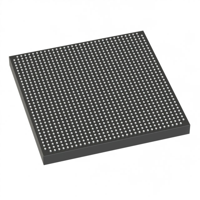
Stratix® V GX Field Programmable Gate Array (FPGA) IC 600 19456000 340000 1152-BBGA, FCBGA |
|---|---|
| Quantity | 1,387 Available (as of June 13, 2026) |

| Product Category | Field Programmable Gate Array (FPGA) |
|---|---|
| Manufacturer | Intel |
| Manufacturing Status | Obsolete |
| Manufacturer Standard Lead Time | Contact Us |
| Datasheet |
Specifications & Environmental
| Device Package | 1152-FBGA (35x35) | Grade | Commercial | Operating Temperature | 0°C – 85°C | ||
|---|---|---|---|---|---|---|---|
| Package / Case | 1152-BBGA, FCBGA | Number of I/O | 600 | Voltage | 870 mV - 930 mV | ||
| Mounting Method | Surface Mount | RoHS Compliance | RoHS Compliant | REACH Compliance | REACH Unknown | ||
| Moisture Sensitivity Level | 3 (168 Hours) | Number of LABs/CLBs | 128300 | Number of Logic Elements/Cells | 340000 | ||
| Number of Gates | N/A | ECCN | 3A001A2C | HTS Code | 8542.39.0001 | ||
| Qualification | N/A | Total RAM Bits | 19456000 |
Overview of 5SGXMA3K3F35C2N – Stratix® V GX Field Programmable Gate Array (FPGA) IC, 1152‑BBGA
The 5SGXMA3K3F35C2N is a Stratix V GX family FPGA from Intel, delivered in a 1152‑BBGA (1152‑FBGA, 35×35) surface‑mount package for commercial applications. It combines high logic density, substantial embedded memory, and extensive I/O to address complex digital processing, communications, and high‑I/O integration tasks.
Designed as part of the Stratix V device family, this GX device aligns with device datasheet characteristics for transceiver, core and periphery switching, and I/O timing as defined for Stratix V GX devices.
Key Features
- Logic Capacity Approximately 340,000 logic elements for implementing large-scale custom digital functions.
- Embedded Memory Approximately 19.46 Mbits of on‑chip RAM to support buffering, FIFOs, and intermediate storage without external memory.
- I/O Density 600 I/O pins providing broad external connectivity for interfaces, peripherals, and board‑level integration.
- Power Supply Validated core supply range of 870 mV to 930 mV to match system power domain requirements described for the device.
- Package & Mounting 1152‑BBGA / 1152‑FBGA (35×35) footprint; surface‑mount package suitable for compact, high‑density PCBs.
- Operating Grade & Temperature Commercial grade with an operating temperature range of 0 °C to 85 °C.
- Series Capabilities Stratix V GX family device characteristics include documented transceiver and I/O timing features in the Stratix V datasheet.
- Regulatory RoHS compliant.
Typical Applications
- Communications & Networking High I/O count and Stratix V GX family transceiver capabilities make this device suitable for network interface functions and protocol bridging in commercial systems.
- High‑Density Digital Processing Large logic element count and on‑chip RAM support complex custom logic, packet processing, and control plane implementations.
- Prototyping & Systems Integration The 1152‑BBGA package and broad I/O enable integration into evaluation platforms and dense system boards for proof‑of‑concept and product development.
Unique Advantages
- High logic density: Approximately 340,000 logic elements reduce the need for multiple devices and simplify system partitioning.
- Substantial embedded memory: About 19.46 Mbits of on‑chip RAM lowers dependence on external memory for intermediate storage and buffering.
- Extensive I/O: 600 I/Os provide flexibility for interfacing multiple peripherals, high‑pin‑count connectors, and board‑level routing.
- Commercial temperature suitability: Rated 0 °C to 85 °C for use in commercial environments where that temperature range is required.
- Compact package: 1152‑FBGA (35×35) surface‑mount package enables dense PCB designs while maintaining high pin count.
- Standards‑aligned family features: As a Stratix V GX device, it adheres to the family’s defined electrical and switching characteristics, including transceiver and I/O timing capabilities documented in the datasheet.
Why Choose 5SGXMA3K3F35C2N?
The 5SGXMA3K3F35C2N positions itself as a high‑capacity, commercially graded FPGA for designs that require substantial logic resources, on‑chip memory, and a large number of I/Os in a compact BGA package. It is well suited for engineers developing complex digital systems, communications interfaces, and high‑integration boards where on‑chip resources and package density matter.
Backed by the Stratix V family specifications, this device offers predictable electrical and switching characteristics for integration into commercial products and development platforms, providing a clear path for scalable designs that leverage Intel’s Stratix V device documentation.
Request a quote or submit a pricing and availability inquiry to evaluate 5SGXMA3K3F35C2N for your next design.


Date Founded: 1968
Headquarters: Santa Clara, California, USA
Employees: 130,000+
Revenue: $54.23 Billion
Certifications and Memberships: ISO9001:2015, ISO14001:2015, ISO17025:2017, ISO27001:2022, ISO45001:2018, ISO50001:2018


