
5SGXMA3K3F35C2LN
| Part Description |
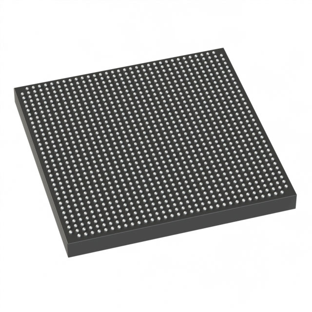
Stratix® V GX Field Programmable Gate Array (FPGA) IC 600 19456000 340000 1152-BBGA, FCBGA |
|---|---|
| Quantity | 1,709 Available (as of June 15, 2026) |

| Product Category | Field Programmable Gate Array (FPGA) |
|---|---|
| Manufacturer | Intel |
| Manufacturing Status | Obsolete |
| Manufacturer Standard Lead Time | Contact Us |
| Datasheet |
Specifications & Environmental
| Device Package | 1152-FBGA (35x35) | Grade | Commercial | Operating Temperature | 0°C – 85°C | ||
|---|---|---|---|---|---|---|---|
| Package / Case | 1152-BBGA, FCBGA | Number of I/O | 600 | Voltage | 820 mV - 880 mV | ||
| Mounting Method | Surface Mount | RoHS Compliance | RoHS Compliant | REACH Compliance | REACH Unknown | ||
| Moisture Sensitivity Level | 3 (168 Hours) | Number of LABs/CLBs | 128300 | Number of Logic Elements/Cells | 340000 | ||
| Number of Gates | N/A | ECCN | 3A001A2C | HTS Code | 8542.39.0001 | ||
| Qualification | N/A | Total RAM Bits | 19456000 |
Overview of 5SGXMA3K3F35C2LN – Stratix® V GX FPGA, 600 I/O, 340,000 logic elements
The 5SGXMA3K3F35C2LN is a Stratix® V GX field programmable gate array (FPGA) provided in a 1152-BBGA (FCBGA) package. It delivers high-density programmable logic, substantial on-chip memory, and a large I/O count for complex digital designs.
Designed for commercial applications, this device targets high-performance communication, signal processing, and system-integration tasks where large logic capacity, abundant embedded memory, and flexible I/O are required.
Key Features
- Logic Capacity Approximately 340,000 logic elements to implement large-scale digital designs and complex custom logic.
- Embedded Memory Approximately 19.5 Mbits of on-chip RAM for buffering, FIFOs, and intermediate data storage in compute and streaming applications.
- I/O Resources Up to 600 general-purpose I/O pins to support dense external interfacing and multi-channel connectivity.
- Transceiver/Series Capabilities Part of the Stratix V family; series documentation specifies GX transceiver speed grades (series-level) that support multi-gigabit channel operation as defined in the device datasheet.
- Power and Core Voltage Core voltage supply range 820 mV to 880 mV, enabling designs that follow the device’s specified power rails.
- Package 1152-BBGA (FCBGA) package; supplier package listed as 1152-FBGA (35 × 35 mm) for high I/O density and compact board footprint.
- Operating Range Commercial temperature grade with an operating temperature range of 0 °C to 85 °C.
- Compliance RoHS compliant.
Typical Applications
- High‑performance networking and communications Leverages the Stratix V family’s transceiver capabilities and high logic density for packet processing, line card, and protocol acceleration tasks.
- Signal processing and DSP Large logic resources and ~19.5 Mbits of embedded memory support complex signal-chain implementations and real‑time processing.
- System integration and prototyping 600 I/O and the 1152-BBGA package allow dense peripheral connectivity for prototyping multi-board or mixed-signal systems.
- Commercial embedded systems Commercial temperature rating (0 °C to 85 °C) aligns with a broad set of embedded applications requiring significant programmable logic and memory.
Unique Advantages
- High logic density: The device’s approximately 340,000 logic elements enable implementation of large, complex designs without immediate need for external logic.
- Substantial on-chip memory: Approximately 19.5 Mbits of embedded RAM reduce dependence on external memory for buffering and intermediate storage.
- Extensive I/O count: Up to 600 I/Os support multi-channel interfacing, parallel buses, and dense peripheral connections on compact PCBs.
- Compact, high-density packaging: The 1152-BBGA (35 × 35 mm) package balances high I/O and board area efficiency for space-constrained designs.
- Commercial readiness: Commercial temperature grade and RoHS compliance simplify integration into mainstream product designs and supply chains.
- Series-level transceiver capability: As a Stratix V GX device, the family’s documented transceiver speed grades support multi‑gigabit channel deployment where applicable per series datasheet.
Why Choose 5SGXMA3K3F35C2LN?
The 5SGXMA3K3F35C2LN combines large-scale programmable logic, substantial embedded memory, and a high I/O count in a compact 1152-BBGA package for commercial embedded and communications designs. Its voltage supply range and commercial temperature rating make it a fit for systems that require a dense, high-capacity FPGA while adhering to typical commercial operating conditions.
This device is suitable for design teams and integrators who need scalable logic capacity, significant on-chip RAM, and flexible interfacing in a single FPGA platform backed by the Stratix V family documentation.
Request a quote or submit an inquiry to receive pricing and availability for 5SGXMA3K3F35C2LN and to discuss how this Stratix V GX FPGA can meet your project requirements.


Date Founded: 1968
Headquarters: Santa Clara, California, USA
Employees: 130,000+
Revenue: $54.23 Billion
Certifications and Memberships: ISO9001:2015, ISO14001:2015, ISO17025:2017, ISO27001:2022, ISO45001:2018, ISO50001:2018


