
5SGXMA4H1F35C2G
| Part Description |
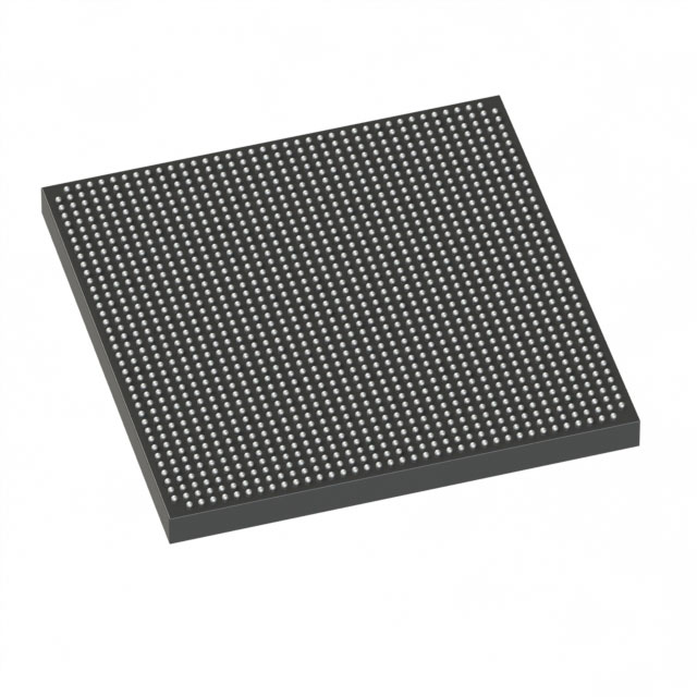
Stratix® V GX Field Programmable Gate Array (FPGA) IC 600 37888000 420000 1152-BBGA, FCBGA |
|---|---|
| Quantity | 148 Available (as of June 19, 2026) |

| Product Category | Field Programmable Gate Array (FPGA) |
|---|---|
| Manufacturer | Intel |
| Manufacturing Status | Active |
| Manufacturer Standard Lead Time | 26 Weeks |
| Datasheet |
Specifications & Environmental
| Device Package | 1152-FBGA (35x35) | Grade | Commercial | Operating Temperature | 0°C – 85°C | ||
|---|---|---|---|---|---|---|---|
| Package / Case | 1152-BBGA, FCBGA | Number of I/O | 600 | Voltage | 870 mV - 930 mV | ||
| Mounting Method | Surface Mount | RoHS Compliance | RoHS Compliant | REACH Compliance | REACH Unaffected | ||
| Moisture Sensitivity Level | 3 (168 Hours) | Number of LABs/CLBs | 158500 | Number of Logic Elements/Cells | 420000 | ||
| Number of Gates | N/A | ECCN | N/A | HTS Code | N/A | ||
| Qualification | N/A | Total RAM Bits | 37888000 |
Overview of 5SGXMA4H1F35C2G – Stratix® V GX FPGA, 420,000 logic elements, 600 I/Os
The 5SGXMA4H1F35C2G is a Stratix V GX field programmable gate array (FPGA) IC in a 1152-BBGA FCBGA package offering high logic density and a large I/O count. As a commercial-grade Stratix V GX device, it delivers significant on-chip memory and logic resources alongside a wide I/O complement for complex, high‑density digital designs.
Designed for applications that require substantial embedded memory, extensive I/O connectivity, and fine-grained core power control, this device provides the building blocks for scalable, performance‑oriented FPGA designs within the specified commercial operating range.
Key Features
- Logic Capacity Provides 420,000 logic elements, enabling implementation of large-scale digital logic networks and complex custom functions.
- Embedded Memory Approximately 37.9 Mbits of on-chip RAM to support buffering, state storage, and memory‑intensive logic functions.
- I/O Density Up to 600 user I/Os to consolidate multiple interfaces and reduce board-level interconnect complexity.
- Transceiver Family Part of the Stratix V GX family; Stratix V GX/GS series datasheet lists GX transceiver speed grade options (e.g., GX channel—14.1 Gbps and 12.5 Gbps) for designs requiring high-speed serial links.
- Power and Core Voltage Core supply range specified from 870 mV to 930 mV, allowing designers to plan power delivery and optimize core operation within the defined window.
- Commercial Temperature Grade Rated for 0 °C to 85 °C operation for applications targeting commercial environments.
- Packaging & Mounting 1152‑BBGA (FCBGA) package with supplier device package listed as 1152‑FBGA (35×35); surface-mount mounting type for compact board layouts.
- Standards & Compliance RoHS‑compliant, supporting regulatory-driven manufacturing and material selection.
Typical Applications
- High-density digital processing: Use the large logic element count and embedded RAM to implement complex signal processing, packet processing, or custom compute blocks.
- Multi-interface bridging and aggregation: High I/O count enables consolidation of parallel and serial interfaces, reducing external glue logic and PCB complexity.
- Memory‑intensive FPGA functions: Approximately 37.9 Mbits of on-chip RAM supports buffering, FIFOs, and state machines for real-time data handling.
Unique Advantages
- High logic density: 420,000 logic elements provide the capacity to implement large, integrated digital systems on a single device.
- Large I/O complement: 600 I/Os simplify system integration by accommodating multiple interfaces without extensive external multiplexing.
- Substantial on-chip memory: Approximately 37.9 Mbits of embedded RAM reduces reliance on external memory for many buffering and state storage needs.
- Commercial-grade specification: Designed for 0 °C to 85 °C operation, matching typical commercial application environments.
- Package options for dense boards: 1152‑BBGA FCBGA (35×35) enables compact, high‑density PCB layouts suitable for space-constrained designs.
- RoHS compliant: Supports environmentally driven manufacturing requirements.
Why Choose 5SGXMA4H1F35C2G?
The 5SGXMA4H1F35C2G positions itself as a high‑capacity commercial Stratix V GX FPGA suited for designs that need abundant logic resources, significant embedded memory, and extensive I/O. Its defined core voltage range and commercial temperature rating allow engineering teams to plan power and thermal management within standard commercial system envelopes.
Choose this device when you require a single‑chip solution to consolidate complex digital functions, deliver memory‑heavy workloads, and support large interface counts while maintaining RoHS compliance and a compact FCBGA footprint.
Request a quote or submit an order inquiry to receive pricing and availability information for the 5SGXMA4H1F35C2G. Our team can provide technical and procurement support to help integrate this Stratix V GX FPGA into your design.


Date Founded: 1968
Headquarters: Santa Clara, California, USA
Employees: 130,000+
Revenue: $54.23 Billion
Certifications and Memberships: ISO9001:2015, ISO14001:2015, ISO17025:2017, ISO27001:2022, ISO45001:2018, ISO50001:2018


