
5SGXMA5H1F35C1G
| Part Description |
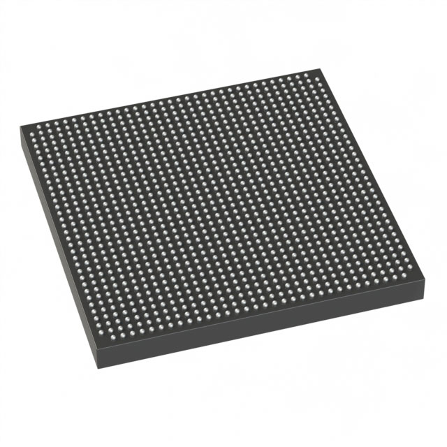
Stratix® V GX Field Programmable Gate Array (FPGA) IC 552 46080000 490000 1152-BBGA, FCBGA |
|---|---|
| Quantity | 155 Available (as of June 15, 2026) |

| Product Category | Field Programmable Gate Array (FPGA) |
|---|---|
| Manufacturer | Intel |
| Manufacturing Status | Active |
| Manufacturer Standard Lead Time | 26 Weeks |
| Datasheet |
Specifications & Environmental
| Device Package | 1152-FBGA (35x35) | Grade | Commercial | Operating Temperature | 0°C – 85°C | ||
|---|---|---|---|---|---|---|---|
| Package / Case | 1152-BBGA, FCBGA | Number of I/O | 552 | Voltage | 870 mV - 930 mV | ||
| Mounting Method | Surface Mount | RoHS Compliance | RoHS Compliant | REACH Compliance | REACH Unaffected | ||
| Moisture Sensitivity Level | 3 (168 Hours) | Number of LABs/CLBs | 185000 | Number of Logic Elements/Cells | 490000 | ||
| Number of Gates | N/A | ECCN | N/A | HTS Code | N/A | ||
| Qualification | N/A | Total RAM Bits | 46080000 |
Overview of 5SGXMA5H1F35C1G – Stratix® V GX Field Programmable Gate Array (1152‑BBGA, 35×35 FCBGA)
The 5SGXMA5H1F35C1G is a commercial‑grade Stratix V GX Field Programmable Gate Array from Intel, offered in a 1152‑ball BGA (FCBGA) package with a 35×35 supplier footprint. It combines high logic density, substantial on‑chip memory, and a large I/O count to address demanding system‑level integration needs.
Engineered for applications that require large numbers of logic elements and embedded memory, this device is suitable for high‑performance digital processing, protocol bridging, and complex system integration where a compact surface‑mount FCBGA package is required.
Key Features
- High Logic Capacity — 490,000 logic elements (cells) to implement extensive combinational and sequential logic structures.
- Embedded Memory — Approximately 46.08 Mbits of total on‑chip RAM for buffering, FIFOs, and on‑device data storage.
- abundant I/O — 552 device I/O pins to support wide parallel interfaces and multiple peripheral connections.
- Package and Mounting — 1152‑BBGA (FCBGA) package; supplier device package specified as 1152‑FBGA (35×35); surface‑mount mounting type for standard PCB assembly.
- Supply and Operating Conditions — Core supply voltage range 870 mV to 930 mV; commercial operating temperature range 0 °C to 85 °C.
- Commercial Grade — Specified as a commercial temperature grade device for designs targeting commercial deployments.
- Family‑Level Transceiver Capability (Stratix V GX) — As part of the Stratix V GX family (device‑level documentation), the family supports GX transceiver speed grades documented in the device datasheet.
- Environmental Compliance — RoHS compliant to meet lead‑free assembly and regulatory requirements.
Typical Applications
- High‑Performance Digital Processing — Implement wide datapaths, custom accelerators, and complex pipelined logic using the device’s large logic element count and embedded RAM.
- Protocol Conversion and Bridging — Use abundant I/O and on‑chip memory to implement multi‑lane protocol bridges and interface adaptation.
- Telecommunications and Networking Subsystems — Integrate packet processing, buffering, and peripheral control functions requiring high logic density and substantial on‑chip RAM.
- Compact System Integration — Leverage the 1152‑BBGA FCBGA package for board space‑constrained deployments that still require high gate count and many I/Os.
Unique Advantages
- Large Logic Fabric — 490,000 logic elements provide the capacity to consolidate multiple functions into a single FPGA, simplifying system architecture.
- Significant On‑Chip Memory — Approximately 46.08 Mbits of embedded RAM reduces external memory dependence for buffers and temporary storage.
- Extensive I/O Count — 552 I/O pins enable integration of broad peripheral sets and high‑bandwidth parallel interfaces without multiplexing compromises.
- Compact BGA Packaging — 1152‑BBGA (35×35) FCBGA lets you achieve high integration in compact form factors suitable for surface‑mount assembly.
- Defined Operating Envelope — Commercial temperature rating (0 °C to 85 °C) and explicit core supply range (870–930 mV) simplify power and thermal planning.
- Manufacturer Support — Part of the Intel Stratix V GX family with published electrical and switching characteristics in the device datasheet for design‑level reference.
Why Choose 5SGXMA5H1F35C1G?
The 5SGXMA5H1F35C1G delivers high logic density, substantial embedded memory, and a large I/O complement in a compact FCBGA package, making it suitable for commercial designs that require consolidation of complex digital functions. Its defined supply and temperature specifications help streamline board‑level power and thermal design.
Designed for engineering teams needing a high‑capacity Stratix V GX FPGA from a major manufacturer, this device is appropriate for projects emphasizing integration, on‑chip buffering, and extensive interfacing in commercial temperature environments.
Request a quote or submit a procurement inquiry to get pricing and lead‑time information for the 5SGXMA5H1F35C1G.


Date Founded: 1968
Headquarters: Santa Clara, California, USA
Employees: 130,000+
Revenue: $54.23 Billion
Certifications and Memberships: ISO9001:2015, ISO14001:2015, ISO17025:2017, ISO27001:2022, ISO45001:2018, ISO50001:2018


