
5SGXMA5K3F35C2N
| Part Description |
Stratix® V GX Field Programmable Gate Array (FPGA) IC 432 46080000 490000 1152-BBGA, FCBGA |
|---|---|
| Quantity | 1,376 Available (as of June 15, 2026) |

| Product Category | Field Programmable Gate Array (FPGA) |
|---|---|
| Manufacturer | Intel |
| Manufacturing Status | Obsolete |
| Manufacturer Standard Lead Time | Contact Us |
| Datasheet |
Specifications & Environmental
| Device Package | 1152-FBGA (35x35) | Grade | Commercial | Operating Temperature | 0°C – 85°C | ||
|---|---|---|---|---|---|---|---|
| Package / Case | 1152-BBGA, FCBGA | Number of I/O | 432 | Voltage | 870 mV - 930 mV | ||
| Mounting Method | Surface Mount | RoHS Compliance | RoHS Compliant | REACH Compliance | REACH Unknown | ||
| Moisture Sensitivity Level | 3 (168 Hours) | Number of LABs/CLBs | 185000 | Number of Logic Elements/Cells | 490000 | ||
| Number of Gates | N/A | ECCN | 3A001A2C | HTS Code | 8542.39.0001 | ||
| Qualification | N/A | Total RAM Bits | 46080000 |
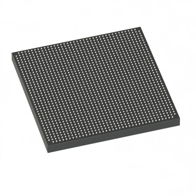
Overview of 5SGXMA5K3F35C2N – Stratix® V GX FPGA, 490,000 logic elements, 1152‑BBGA
The 5SGXMA5K3F35C2N is a Stratix® V GX field‑programmable gate array (FPGA) IC optimized for high‑density, I/O‑rich designs. It combines a large logic fabric with substantial embedded RAM and a commercial operating grade to support complex digital processing, system integration, and I/O interfacing.
Key value propositions include high logic capacity, approximately 46 Mbits of embedded memory, and a compact 1152‑ball FCBGA package suited for surface‑mount assembly in commercial electronic systems.
Key Features
- Logic Capacity — 490,000 logic elements and 185,000 logic blocks, enabling large, deeply pipelined or highly parallel digital designs.
- Embedded Memory — Approximately 46 Mbits of on‑chip RAM for buffering, lookup tables, and on‑chip storage without external memory dependency.
- I/O Density — 432 user I/O pins to support high channel counts, extensive peripheral interfacing, and complex board routing.
- Power and Core Supply — Core voltage specified at 870 mV to 930 mV for the device core supply range.
- Package and Mounting — 1152‑BBGA FCBGA package (supplier device package: 1152‑FBGA, 35×35) designed for surface‑mount applications.
- Operating Grade — Commercial temperature range rated from 0 °C to 85 °C for standard commercial deployments.
- Environmental Compliance — RoHS compliant.
- Series Characteristics (Stratix V GX) — Part of the Stratix V GX family; series datasheet documents electrical and switching characteristics including transceiver and I/O timing details for system integration and high‑speed channel support.
Typical Applications
- Communications and Networking — High logic density and abundant I/O make this device suitable for I/O‑intensive protocol processing and interface aggregation.
- High‑Performance Signal Processing — Large logic resources and on‑chip RAM support parallel DSP pipelines and custom processing engines.
- Data Center and Compute Acceleration — Use in programmable acceleration functions where large logic and embedded memory enable application‑specific compute offload.
- Complex System Integration — High I/O count and extensive logic permit consolidation of multiple functions onto a single FPGA for board‑level integration.
Unique Advantages
- High logic density: 490,000 logic elements deliver capacity for complex state machines, compute kernels, and large custom datapaths.
- Substantial on‑chip memory: Approximately 46 Mbits of embedded RAM reduces reliance on external memory and improves latency for buffering and lookup operations.
- Generous I/O resources: 432 user I/Os support multi‑lane interfaces and rich peripheral connectivity without external multiplexing.
- Compact, production‑ready package: 1152‑BBGA (35×35) FCBGA in a surface‑mount form factor for dense board layouts and automated assembly.
- Commercial temperature rating: Specified 0 °C to 85 °C operation for standard commercial electronics applications.
- Regulatory readiness: RoHS compliance simplifies environmental and supply‑chain considerations.
Why Choose 5SGXMA5K3F35C2N?
The 5SGXMA5K3F35C2N positions itself as a high‑capacity, I/O‑rich Stratix V GX FPGA suitable for demanding commercial designs that require substantial logic resources and on‑chip memory. Its package, power envelope, and I/O complement make it appropriate for integrators seeking to consolidate complex digital functions and accelerate custom processing tasks.
Design teams targeting scalable, programmable solutions will find the combination of logic elements, embedded RAM, and I/O density advantageous for reducing external component count and simplifying board-level architecture while maintaining commercial operating requirements.
If you would like pricing, availability, or a formal quote for 5SGXMA5K3F35C2N, request a quote or submit an inquiry to our sales team and include your quantity, required lead time, and any application notes relevant to your design. We’ll respond with tailored procurement and technical support information.


Date Founded: 1968
Headquarters: Santa Clara, California, USA
Employees: 130,000+
Revenue: $54.23 Billion
Certifications and Memberships: ISO9001:2015, ISO14001:2015, ISO17025:2017, ISO27001:2022, ISO45001:2018, ISO50001:2018


