
5SGXMA5K3F35C2WN
| Part Description |
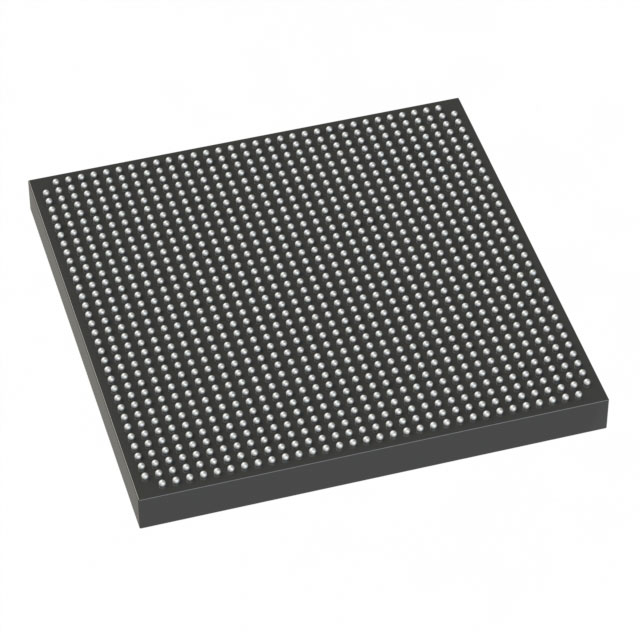
Stratix® V GX Field Programmable Gate Array (FPGA) IC 432 46080000 490000 1152-BBGA, FCBGA |
|---|---|
| Quantity | 1,511 Available (as of June 14, 2026) |

| Product Category | Field Programmable Gate Array (FPGA) |
|---|---|
| Manufacturer | Intel |
| Manufacturing Status | Obsolete |
| Manufacturer Standard Lead Time | Contact Us |
| Datasheet |
Specifications & Environmental
| Device Package | 1152-FBGA (35x35) | Grade | Commercial | Operating Temperature | 0°C – 85°C | ||
|---|---|---|---|---|---|---|---|
| Package / Case | 1152-BBGA, FCBGA | Number of I/O | 432 | Voltage | 870 mV - 930 mV | ||
| Mounting Method | Surface Mount | RoHS Compliance | RoHS non-compliant | REACH Compliance | REACH Unknown | ||
| Moisture Sensitivity Level | 4 (72 Hours) | Number of LABs/CLBs | 185000 | Number of Logic Elements/Cells | 490000 | ||
| Number of Gates | N/A | ECCN | OBSOLETE | HTS Code | N/A | ||
| Qualification | N/A | Total RAM Bits | 46080000 |
Overview of 5SGXMA5K3F35C2WN – Stratix® V GX Field Programmable Gate Array (FPGA) IC, 490,000 logic elements
The 5SGXMA5K3F35C2WN is a Stratix V GX family FPGA offering a high-density programmable logic fabric and substantial on-chip memory for complex digital designs. This commercial-grade device provides 490,000 logic elements and approximately 46 Mbits of embedded RAM, along with 432 I/O pins and a 1152-ball FCBGA package for compact, high-pin-count board implementations.
Designed for applications that require large logic capacity and significant on-chip memory, this FPGA balances integration and board-level I/O density while operating within a core voltage range of 870 mV to 930 mV and a commercial temperature range of 0 °C to 85 °C.
Key Features
- Core Logic 490,000 logic elements provide extensive programmable logic resources for complex data-paths and control logic.
- Embedded Memory Approximately 46 Mbits of on-chip RAM to support large buffers, FIFOs, and state machines without external memory.
- I/O Capacity 432 user I/O pins for high-density interfacing to peripherals, transceivers, and board-level buses.
- Power and Voltage Core supply defined at 870 mV to 930 mV, enabling predictable power planning for system designs.
- Package and Mounting 1152-BBGA / 1152-FBGA (35×35) FCBGA package, surface-mountable for compact, high-pin-count PCB layouts.
- Operating Grade & Temperature Commercial grade with an operating temperature range of 0 °C to 85 °C.
- Regulatory Compliance RoHS compliant for lead-free assembly and regulatory alignment in commercial products.
Typical Applications
- High-density digital processing — Implement large custom datapaths, signal processing pipelines, and parallel compute kernels using the device's 490,000 logic elements and embedded RAM.
- Network and packet processing — Use abundant on-chip memory and extensive I/O to build packet buffers, classification engines, and protocol handlers.
- Prototyping and system emulation — Consolidate logic and memory for hardware prototypes, FPGA-based validation, and pre-silicon verification tasks.
- Board-level integration — Leverage 432 I/Os and the 1152-ball FCBGA package for densely connected, compact system boards.
Unique Advantages
- High logic capacity: 490,000 logic elements enable complex and large-scale designs without partitioning across multiple devices.
- Substantial on-chip memory: Approximately 46 Mbits of embedded RAM reduces dependency on external memory for many buffering and caching needs.
- Generous I/O resources: 432 I/Os provide flexible connectivity for parallel interfaces, high-pin-count peripherals, and multi-channel systems.
- Compact, manufacturable package: 1152-ball FCBGA (35×35) package supports surface-mount assembly for dense PCB integration.
- Commercial-grade operating window: Rated for 0 °C to 85 °C with defined core voltage range for consistent system-level power design.
- RoHS compliant: Aligns with lead-free manufacturing requirements for commercial products.
Why Choose 5SGXMA5K3F35C2WN?
The 5SGXMA5K3F35C2WN positions itself as a high-density Stratix V GX FPGA option for engineers who need large programmable logic capacity combined with significant embedded memory and substantial I/O. Its FCBGA package and surface-mount form factor make it suitable for compact, high-pin-count boards while the defined core voltage and commercial temperature range simplify power and thermal planning.
This device is well suited to teams developing complex digital systems, network processing functions, or hardware prototypes that require consolidated logic and memory resources in a single commercial-grade FPGA. Its RoHS compliance further supports integration into modern commercial product lines.
Request a quote or submit an inquiry to receive pricing and availability information for 5SGXMA5K3F35C2WN.


Date Founded: 1968
Headquarters: Santa Clara, California, USA
Employees: 130,000+
Revenue: $54.23 Billion
Certifications and Memberships: ISO9001:2015, ISO14001:2015, ISO17025:2017, ISO27001:2022, ISO45001:2018, ISO50001:2018


