
5SGXMA5N2F45C3G
| Part Description |
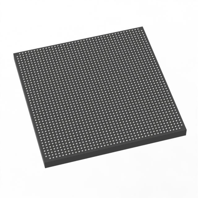
Stratix® V GX Field Programmable Gate Array (FPGA) IC 840 46080000 490000 1932-BBGA, FCBGA |
|---|---|
| Quantity | 1,647 Available (as of June 14, 2026) |
| Product Category | Field Programmable Gate Array (FPGA) |
|---|---|
| Manufacturer | Intel |
| Manufacturing Status | Active |
| Manufacturer Standard Lead Time | 26 Weeks |
| Datasheet |
Specifications & Environmental
| Device Package | 1932-FBGA, FC (45x45) | Grade | Commercial | Operating Temperature | 0°C – 85°C | ||
|---|---|---|---|---|---|---|---|
| Package / Case | 1932-BBGA, FCBGA | Number of I/O | 840 | Voltage | 820 mV - 880 mV | ||
| Mounting Method | Surface Mount | RoHS Compliance | RoHS Compliant | REACH Compliance | REACH Unaffected | ||
| Moisture Sensitivity Level | 3 (168 Hours) | Number of LABs/CLBs | 185000 | Number of Logic Elements/Cells | 490000 | ||
| Number of Gates | N/A | ECCN | N/A | HTS Code | N/A | ||
| Qualification | N/A | Total RAM Bits | 46080000 |
Overview of 5SGXMA5N2F45C3G – Stratix® V GX Field Programmable Gate Array (FPGA) IC, 1932-BBGA FCBGA
The 5SGXMA5N2F45C3G is a Stratix V GX family FPGA in a 1932-ball BGA FCBGA package, offered in a commercial temperature grade. It delivers very large programmable logic capacity with extensive I/O and embedded memory, intended for designs that require high integration and significant on-chip resources.
As a Stratix V GX device, it belongs to a device family documented for electrical and high-speed switching characteristics in the Stratix V device datasheet, including family-level transceiver speed grade options.
Key Features
- Logic Capacity Contains 490,000 logic elements suitable for large-scale programmable logic implementations.
- Embedded Memory Approximately 46.08 Mbits of total on-chip RAM to support buffering, state storage, and data processing.
- I/O Density 840 user I/O pins to support high-pin-count interfaces and complex board-level connectivity.
- Package & Mounting 1932-ball BGA (FCBGA) package; supplier device package listed as 1932-FBGA, FC (45×45). Surface-mount construction.
- Power Supply Core voltage supply range: 820 mV to 880 mV, enabling designs that target specified core power rails.
- Temperature Grade Commercial operating temperature range of 0 °C to 85 °C as specified for this part.
- RoHS Compliance Device is RoHS compliant.
- Stratix V GX Family Characteristics As a member of the Stratix V GX family, the series documentation includes transceiver speed grade options and detailed electrical and switching specifications in the family datasheet.
Typical Applications
- High-density logic systems Designs that require large programmable logic capacity and complex custom logic implementations.
- On-chip buffering and memory-heavy designs Applications that need substantial embedded RAM for data buffering, packet queues, or state storage.
- High-pin-count interface boards Systems requiring hundreds of I/O signals for multi-channel connectivity or dense peripheral integration.
Unique Advantages
- Extensive programmable resources: 490,000 logic elements provide a platform for consolidating complex functions into a single device, reducing component count.
- Large on-chip RAM: Approximately 46.08 Mbits of embedded memory helps minimize external memory dependence and simplifies board design.
- High I/O availability: 840 I/Os enable flexible interfacing to multiple subsystems without extensive multiplexing or external interface chips.
- Compact, surface-mount package: 1932-BBGA FCBGA packaging offers high density in a single-package solution suitable for compact system boards.
- Standards-based compliance: RoHS compliance supports environmental and regulatory requirements for lead-free assembly.
Why Choose 5SGXMA5N2F45C3G?
The 5SGXMA5N2F45C3G combines very large logic capacity, substantial embedded memory, and a high I/O count in a single Stratix V GX FCBGA package. Its commercial temperature rating and defined core voltage range make it a clear choice for designs that require consolidated programmable logic and memory resources while maintaining clear electrical and thermal operating bounds.
This part is well suited to teams implementing large-scale FPGA designs where integration density, on-chip RAM, and I/O capacity drive system architecture decisions. The Stratix V family documentation provides detailed electrical and transceiver characteristics to support design verification and system integration.
Request a quote or submit an inquiry for 5SGXMA5N2F45C3G to receive pricing and availability information for your design requirements.


Date Founded: 1968
Headquarters: Santa Clara, California, USA
Employees: 130,000+
Revenue: $54.23 Billion
Certifications and Memberships: ISO9001:2015, ISO14001:2015, ISO17025:2017, ISO27001:2022, ISO45001:2018, ISO50001:2018


