
5SGXMA7H3F35C3WN
| Part Description |
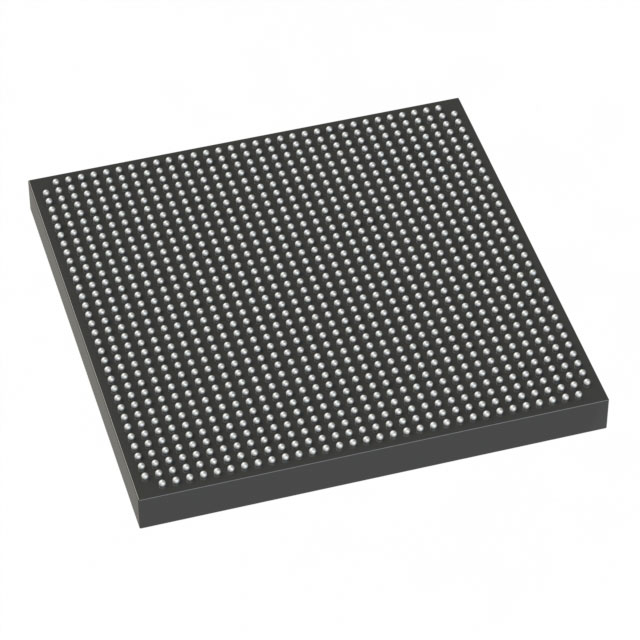
Stratix® V GX Field Programmable Gate Array (FPGA) IC 552 51200000 622000 1152-BBGA, FCBGA |
|---|---|
| Quantity | 1,339 Available (as of June 15, 2026) |

| Product Category | Field Programmable Gate Array (FPGA) |
|---|---|
| Manufacturer | Intel |
| Manufacturing Status | Obsolete |
| Manufacturer Standard Lead Time | Contact Us |
| Datasheet |
Specifications & Environmental
| Device Package | 1152-FBGA (35x35) | Grade | Commercial | Operating Temperature | 0°C – 85°C | ||
|---|---|---|---|---|---|---|---|
| Package / Case | 1152-BBGA, FCBGA | Number of I/O | 552 | Voltage | 820 mV - 880 mV | ||
| Mounting Method | Surface Mount | RoHS Compliance | RoHS non-compliant | REACH Compliance | REACH Unknown | ||
| Moisture Sensitivity Level | 4 (72 Hours) | Number of LABs/CLBs | 234720 | Number of Logic Elements/Cells | 622000 | ||
| Number of Gates | N/A | ECCN | OBSOLETE | HTS Code | N/A | ||
| Qualification | N/A | Total RAM Bits | 51200000 |
Overview of 5SGXMA7H3F35C3WN – Stratix® V GX Field Programmable Gate Array (FPGA) IC
The 5SGXMA7H3F35C3WN is a Stratix® V GX family FPGA from Intel, offered in a 1152‑BBGA FCBGA package. It delivers high on‑chip logic and memory resources in a commercial‑grade device, intended for complex digital designs that require substantial logic density and embedded RAM.
Key attributes include 622,000 logic elements, approximately 51.2 Mbits of embedded memory, and 552 dedicated I/O pins, combined with a surface‑mount 1152‑FBGA (35×35) package and a commercial operating range of 0 °C to 85 °C.
Key Features
- Core Capacity Approximately 622,000 logic elements and 234,720 logic array blocks (LABs) for large, compute‑intensive FPGA designs.
- Embedded Memory Approximately 51.2 Mbits of on‑chip RAM to support high‑bandwidth buffering, state storage, and local data processing.
- I/O Density 552 I/O pins to accommodate complex interfaces and multi‑lane connectivity within a single device.
- Power Specified voltage supply range of 820 mV to 880 mV to match platform core voltage requirements.
- Package & Mounting 1152‑BBGA, FCBGA package (supplier package: 1152‑FBGA, 35×35) designed for surface‑mount PCB assembly.
- Temperature & Grade Commercial grade device with an operating temperature range of 0 °C to 85 °C.
- Compliance RoHS compliant.
Typical Applications
- Large‑scale FPGA designs For systems that require high logic density and significant embedded RAM within a single FPGA footprint.
- Complex I/O systems Applications that need hundreds of I/O signals and flexible pin budgeting on a compact package.
- Data buffering and on‑chip processing Designs that leverage substantial embedded memory for intermediate storage and local data handling.
Unique Advantages
- High logic density: 622,000 logic elements enable implementation of large designs without splitting functionality across multiple devices.
- Significant embedded memory: Approximately 51.2 Mbits of on‑chip RAM supports complex buffering and state machines directly on the FPGA.
- Robust I/O count: 552 I/O pins provide flexibility for multi‑interface designs and high‑pin‑count systems.
- Industry standard packaging: 1152‑FBGA (35×35) package in a surface‑mount form factor suitable for typical production assembly flows.
- Commercial temperature rating: Specified 0 °C to 85 °C operating range for mainstream commercial applications.
- Regulatory compliance: RoHS compliant for regulatory and manufacturing consistency.
Why Choose 5SGXMA7H3F35C3WN?
The 5SGXMA7H3F35C3WN positions itself as a high‑capacity Stratix V GX FPGA for commercial applications that demand large logic arrays, abundant embedded memory, and extensive I/O. Its combination of 622,000 logic elements, roughly 51.2 Mbits of on‑chip RAM, and 552 I/Os in a 1152‑FBGA package supports dense, single‑chip implementations of complex digital systems.
Designed and documented within the Intel Stratix V family, this device is suited to engineers and procurement teams specifying commercial‑grade FPGAs where logic capacity, memory resources, and I/O count are primary selection criteria.
Request a quote or submit an inquiry to receive pricing, availability, and lead‑time information for the 5SGXMA7H3F35C3WN.


Date Founded: 1968
Headquarters: Santa Clara, California, USA
Employees: 130,000+
Revenue: $54.23 Billion
Certifications and Memberships: ISO9001:2015, ISO14001:2015, ISO17025:2017, ISO27001:2022, ISO45001:2018, ISO50001:2018


