
5SGXMA7H3F35C4G
| Part Description |
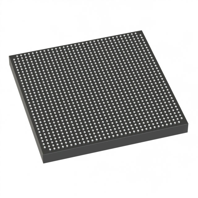
Stratix® V GX Field Programmable Gate Array (FPGA) IC 552 51200000 622000 1152-BBGA, FCBGA |
|---|---|
| Quantity | 1,925 Available (as of June 15, 2026) |

| Product Category | Field Programmable Gate Array (FPGA) |
|---|---|
| Manufacturer | Intel |
| Manufacturing Status | Active |
| Manufacturer Standard Lead Time | 26 Weeks |
| Datasheet |
Specifications & Environmental
| Device Package | 1152-FBGA (35x35) | Grade | Commercial | Operating Temperature | 0°C – 85°C | ||
|---|---|---|---|---|---|---|---|
| Package / Case | 1152-BBGA, FCBGA | Number of I/O | 552 | Voltage | 820 mV - 880 mV | ||
| Mounting Method | Surface Mount | RoHS Compliance | RoHS Compliant | REACH Compliance | REACH Unaffected | ||
| Moisture Sensitivity Level | 3 (168 Hours) | Number of LABs/CLBs | 234720 | Number of Logic Elements/Cells | 622000 | ||
| Number of Gates | N/A | ECCN | N/A | HTS Code | N/A | ||
| Qualification | N/A | Total RAM Bits | 51200000 |
Overview of 5SGXMA7H3F35C4G – Stratix® V GX Field Programmable Gate Array (FPGA) IC 552 51200000 622000 1152-BBGA, FCBGA
The 5SGXMA7H3F35C4G is an Intel Stratix® V GX family FPGA providing high on-chip logic and memory capacity in a high-pin-count FCBGA package. It delivers a combination of large programmable logic resources, substantial embedded RAM, and broad I/O potential suitable for demanding commercial embedded designs.
This device is targeted at applications that require extensive configurable logic, sizable embedded memory, and dense board-level I/O while operating within commercial temperature ranges and low-voltage core supply conditions.
Key Features
- Core Logic — 622,000 logic elements provide substantial programmable logic capacity for complex hardware acceleration and custom datapaths.
- Embedded Memory — Approximately 51.2 Mbits of on-chip RAM to support large buffering, lookup tables, and state storage without external memory for many use cases.
- I/O Density — 552 device I/O pins enable extensive board connectivity and multi-channel interfacing on a single device.
- Power — Core voltage supply range of 820 mV to 880 mV supports the device’s low-voltage core operation requirements.
- Package & Mounting — 1152-BBGA FCBGA (supplier package: 1152-FBGA, 35 × 35 mm) in a surface-mount form factor for high-density board designs.
- Commercial Grade & Temperature — Designed for commercial-grade use with an operating temperature range of 0 °C to 85 °C.
- Regulatory — RoHS compliant.
Typical Applications
- High-density programmable logic — Large logic element counts and embedded RAM make the device suitable for custom hardware acceleration and complex state machines within commercial systems.
- Multi-channel I/O systems — With 552 I/O pins, the FPGA supports designs requiring many parallel interfaces or channelized connectivity at the board level.
- Board-level integration — The 1152-BBGA FCBGA package and surface-mount mounting suit compact, high-density PCB layouts.
- Commercial embedded products — The commercial temperature grade (0 °C to 85 °C) aligns the device with a wide range of commercial electronics and embedded applications.
Unique Advantages
- Substantial on-chip logic capacity: 622,000 logic elements allow consolidation of complex functions into a single FPGA, reducing system-level BOM and inter-chip latency.
- Large embedded memory pool: Approximately 51.2 Mbits of RAM supports deep buffering and on-chip data storage, minimizing reliance on external memory for many designs.
- Extensive I/O capability: 552 I/Os enable broad peripheral and channel integration without sacrificing board real estate for additional interface devices.
- Compact, high-density package: The 1152-BBGA FCBGA (35 × 35 mm) surface-mount package supports dense PCB implementations while delivering high pin count.
- Commercial operating range: Rated for 0 °C to 85 °C to match typical commercial deployment environments.
- Compliance and supply consistency: RoHS compliance and Intel manufacturing provide traceable sourcing and regulatory alignment for commercial products.
Why Choose 5SGXMA7H3F35C4G?
The 5SGXMA7H3F35C4G brings a balance of high logic density, significant on-chip RAM, and substantial I/O in a single Stratix V GX FCBGA package—making it well suited for commercial embedded designs that demand integrated, programmable solutions. Its low-voltage core supply range and surface-mount, high-pin-count package support compact, power-aware board designs.
Designed and manufactured by Intel as part of the Stratix V GX family, this device is a practical choice for engineers seeking a scalable, high-capacity FPGA platform for commercial applications where on-chip resources and I/O density simplify system architecture and reduce external component count.
Request a quote or submit an inquiry for pricing and availability for part number 5SGXMA7H3F35C4G.


Date Founded: 1968
Headquarters: Santa Clara, California, USA
Employees: 130,000+
Revenue: $54.23 Billion
Certifications and Memberships: ISO9001:2015, ISO14001:2015, ISO17025:2017, ISO27001:2022, ISO45001:2018, ISO50001:2018


