
5SGXMA7N2F45I3LN
| Part Description |
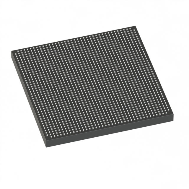
Stratix® V GX Field Programmable Gate Array (FPGA) IC 840 51200000 622000 1932-BBGA, FCBGA |
|---|---|
| Quantity | 145 Available (as of June 15, 2026) |

| Product Category | Field Programmable Gate Array (FPGA) |
|---|---|
| Manufacturer | Intel |
| Manufacturing Status | Obsolete |
| Manufacturer Standard Lead Time | Contact Us |
| Datasheet |
Specifications & Environmental
| Device Package | 1932-FBGA, FC (45x45) | Grade | Industrial | Operating Temperature | -40°C – 100°C | ||
|---|---|---|---|---|---|---|---|
| Package / Case | 1932-BBGA, FCBGA | Number of I/O | 840 | Voltage | 820 mV - 880 mV | ||
| Mounting Method | Surface Mount | RoHS Compliance | RoHS Compliant | REACH Compliance | REACH Unknown | ||
| Moisture Sensitivity Level | 3 (168 Hours) | Number of LABs/CLBs | 234720 | Number of Logic Elements/Cells | 622000 | ||
| Number of Gates | N/A | ECCN | 3A001A2C | HTS Code | 8542.39.0001 | ||
| Qualification | N/A | Total RAM Bits | 51200000 |
Overview of 5SGXMA7N2F45I3LN – Stratix® V GX Field Programmable Gate Array (FPGA), 840 I/O
The 5SGXMA7N2F45I3LN is an Intel Stratix V GX family FPGA in a 1932-ball FCBGA package, offering very large logic capacity and high I/O density for industrial-grade systems. It combines 622,000 logic elements, approximately 51.2 Mbits of embedded memory, and up to 840 I/O to support complex, high-density digital designs.
Designed for surface-mount assembly and rated for industrial temperature operation, this device is suited to applications that require large programmable logic resources, extensive I/O, and a robust thermal/voltage operating window.
Key Features
- High Logic Capacity — 622,000 logic elements to implement large-scale custom logic, datapaths, and control architectures.
- Embedded Memory — Approximately 51.2 Mbits of on-chip RAM for buffering, look-up tables, and state storage within the FPGA fabric.
- High I/O Count — 840 I/O pins to support dense board-level routing and numerous peripheral interfaces.
- Package & Mounting — 1932-BBGA FCBGA package (supplier package: 1932-FBGA, FC, 45×45 mm) optimized for surface-mount assembly.
- Industrial Temperature Grade — Rated for operation from −40 °C to 100 °C for deployment in industrial environments.
- Core Supply Range — Core voltage supply specified from 820 mV to 880 mV for predictable power planning.
- Regulatory Compliance — RoHS compliant.
Typical Applications
- High-density digital processing — Large logic capacity and on-chip memory enable implementation of complex algorithms, packet processing, and custom compute pipelines.
- High I/O systems — The 840 I/O count supports dense peripheral connectivity, multi-channel interfaces, and board-level signal routing.
- Industrial control and automation — Industrial temperature rating and robust package make the device suitable for industrial instrumentation and control systems.
- High-speed serial/transceiver-based designs — Part of the Stratix V GX family (series datasheet information) for applications requiring advanced transceiver capabilities within the family scope.
Unique Advantages
- Large programmable fabric: 622,000 logic elements provide headroom for complex state machines, wide datapaths, and parallel processing blocks, reducing the need for multiple devices.
- Substantial embedded memory: Approximately 51.2 Mbits of RAM on-chip reduces external memory dependence and improves data throughput for buffering and caching tasks.
- Extensive I/O capacity: 840 I/O pins simplify integration of multiple interfaces and sensors without external multiplexing, lowering BOM complexity.
- Industrial-ready thermal range: −40 °C to 100 °C operation supports deployment in demanding environmental conditions.
- Compact, production-ready package: 1932-ball FCBGA (45×45 mm supplier package) in a surface-mount format streamlines manufacturing for high-density boards.
- Standards-compliant supply and materials: RoHS compliance and defined core supply range aid in predictable power design and regulatory alignment.
Why Choose 5SGXMA7N2F45I3LN?
The 5SGXMA7N2F45I3LN offers a balance of very large logic capacity, significant on-chip memory, and high I/O count in an industrial-temperature, surface-mount FCBGA package. It is targeted at engineers building complex, high-density FPGA designs that require substantial programmable resources and robust environmental performance.
Its clear electrical and mechanical parameters—622,000 logic elements, approximately 51.2 Mbits of embedded RAM, 840 I/O, a defined core voltage range, and RoHS compliance—make it straightforward to evaluate for system integration, thermal planning, and long-term deployment in industrial applications.
Request a quote or submit a parts inquiry for 5SGXMA7N2F45I3LN to receive pricing, availability, and technical support for your project.


Date Founded: 1968
Headquarters: Santa Clara, California, USA
Employees: 130,000+
Revenue: $54.23 Billion
Certifications and Memberships: ISO9001:2015, ISO14001:2015, ISO17025:2017, ISO27001:2022, ISO45001:2018, ISO50001:2018


