
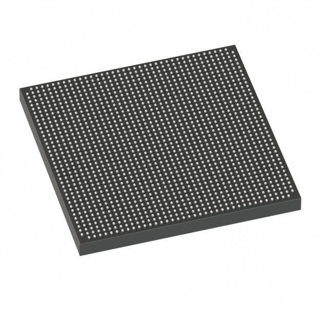
5SGXMA7N3F45C2LG
| Part Description |
Stratix® V GX Field Programmable Gate Array (FPGA) IC 840 51200000 622000 1932-BBGA, FCBGA |
|---|---|
| Quantity | 1,511 Available (as of June 15, 2026) |

| Product Category | Field Programmable Gate Array (FPGA) |
|---|---|
| Manufacturer | Intel |
| Manufacturing Status | Active |
| Manufacturer Standard Lead Time | 26 Weeks |
| Datasheet |
Specifications & Environmental
| Device Package | 1932-FBGA, FC (45x45) | Grade | Commercial | Operating Temperature | 0°C – 85°C | ||
|---|---|---|---|---|---|---|---|
| Package / Case | 1932-BBGA, FCBGA | Number of I/O | 840 | Voltage | 820 mV - 880 mV | ||
| Mounting Method | Surface Mount | RoHS Compliance | RoHS Compliant | REACH Compliance | REACH Unaffected | ||
| Moisture Sensitivity Level | 3 (168 Hours) | Number of LABs/CLBs | 234720 | Number of Logic Elements/Cells | 622000 | ||
| Number of Gates | N/A | ECCN | N/A | HTS Code | N/A | ||
| Qualification | N/A | Total RAM Bits | 51200000 |
Overview of 5SGXMA7N3F45C2LG – Stratix® V GX Field Programmable Gate Array (FPGA) IC, 840 I/O, 622,000 logic elements
The 5SGXMA7N3F45C2LG is a Stratix® V GX Field Programmable Gate Array (FPGA) IC from Intel, offering a high-density programmable fabric in a 1932-BBGA (FCBGA) package. This commercial-grade device provides abundant logic resources, extensive on-chip memory, and a large I/O count for complex digital designs.
Engineered for designs that require significant logic capacity and flexible I/O routing, the device delivers approximately 51.2 Mbits of embedded memory, 622,000 logic elements, and 840 I/Os while operating within a core supply range of 820 mV to 880 mV and a commercial temperature range of 0 °C to 85 °C.
Key Features
- Core Logic 622,000 logic elements provide a high-capacity programmable fabric for complex digital functions and custom accelerators.
- Embedded Memory Approximately 51.2 Mbits of on-chip RAM to support buffering, lookup tables, and memory-intensive algorithms without external memory dependency.
- I/O Density 840 user I/Os enable broad interfacing options for high-pin-count designs and multi-channel connectivity.
- Power Supply Core voltage support from 820 mV to 880 mV allows precise power provisioning for the device’s core logic.
- Package 1932-BBGA (FCBGA) supplier device package noted as 1932-FBGA, FC (45×45) for high-density board integration.
- Commercial Grade & Temperature Rated for commercial operation with an operating temperature range of 0 °C to 85 °C.
- Standards & Compliance RoHS compliant for regulatory alignment in standard commercial applications.
Typical Applications
- High-density programmable logic Use where substantial logic fabric is required—622,000 logic elements support complex state machines, datapaths, and custom compute blocks.
- Memory-intensive processing Approximately 51.2 Mbits of embedded RAM enables on-chip buffering, lookup tables, and data staging for algorithms that require large local memory.
- Multi-channel I/O aggregation With 840 I/Os, the device is suited for designs needing extensive peripheral or parallel interface connectivity.
- System integration in commercial products Commercial temperature rating and RoHS compliance make this device appropriate for industrial and enterprise equipment operating within 0 °C to 85 °C.
Unique Advantages
- High logic capacity: 622,000 logic elements reduce the need for multiple FPGAs by consolidating large designs into a single device.
- Substantial on-chip RAM: Approximately 51.2 Mbits of embedded memory lowers external memory requirements and simplifies board design.
- Extensive I/O count: 840 I/Os provide flexibility to connect many peripherals, channels, or parallel interfaces without external multiplexing.
- Compact, high-density package: 1932-BBGA (45×45) package supports high pin-count integration in a compact footprint for space-constrained boards.
- Commercial readiness: Commercial temperature grade (0 °C to 85 °C) and RoHS compliance support deployment in a wide range of commercial systems.
Why Choose 5SGXMA7N3F45C2LG?
The 5SGXMA7N3F45C2LG positions itself as a high-density Stratix V GX FPGA option for designers who need extensive logic, embedded memory, and I/O resources in a single commercial-grade device. Its combination of 622,000 logic elements, approximately 51.2 Mbits of on-chip RAM, and 840 I/Os enables consolidation of complex functions and simplifies system architecture.
Backed by Intel’s Stratix V family documentation and electrical characterization, this device is suited for development teams and procurement focused on scalable, high-capacity programmable logic solutions that meet commercial operating and regulatory expectations.
Request a quote or submit an inquiry to receive pricing and availability information for the 5SGXMA7N3F45C2LG. Our team will respond with lead time, packaging options, and ordering details.


Date Founded: 1968
Headquarters: Santa Clara, California, USA
Employees: 130,000+
Revenue: $54.23 Billion
Certifications and Memberships: ISO9001:2015, ISO14001:2015, ISO17025:2017, ISO27001:2022, ISO45001:2018, ISO50001:2018


