
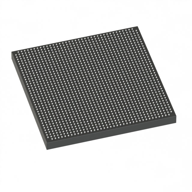
5SGXMABK3H40C2NCV
| Part Description |
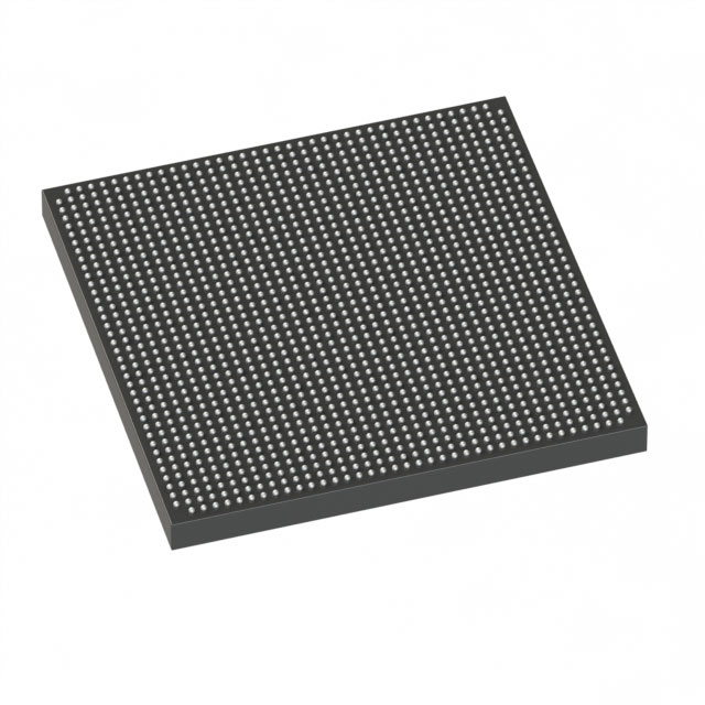
Stratix® V GX Field Programmable Gate Array (FPGA) IC 696 53248000 952000 1517-BBGA, FCBGA |
|---|---|
| Quantity | 1,462 Available (as of October 8, 2026) |
| Product Category | Field Programmable Gate Array (FPGA) |
|---|---|
| Manufacturer | Intel |
| Manufacturing Status | Obsolete |
| Manufacturer Standard Lead Time | Contact Us |
| Datasheet |
Specifications & Environmental
| Device Package | 1517-HBGA (45x45) | Grade | Commercial | Operating Temperature | 0°C – 85°C | ||
|---|---|---|---|---|---|---|---|
| Package / Case | 1517-BBGA, FCBGA | Number of I/O | 696 | Voltage | 870 mV - 930 mV | ||
| Mounting Method | Surface Mount | RoHS Compliance | RoHS non-compliant | REACH Compliance | REACH Unknown | ||
| Moisture Sensitivity Level | 4 (72 Hours) | Number of LABs/CLBs | 359200 | Number of Logic Elements/Cells | 952000 | ||
| Number of Gates | N/A | ECCN | OBSOLETE | HTS Code | N/A | ||
| Qualification | N/A | Total RAM Bits | 53248000 |
Overview of 5SGXMABK3H40C2NCV – Stratix® V GX Field Programmable Gate Array (FPGA), 952,000 logic elements, 696 I/O
The 5SGXMABK3H40C2NCV is a Stratix® V GX Field Programmable Gate Array (FPGA) from Intel, engineered for designs that require very high logic capacity, abundant I/O, and substantial on-chip memory. This commercial-grade FPGA delivers a large programmable fabric and transceiver-capable architecture suitable for designs requiring high integration and performance within a commercial temperature range.
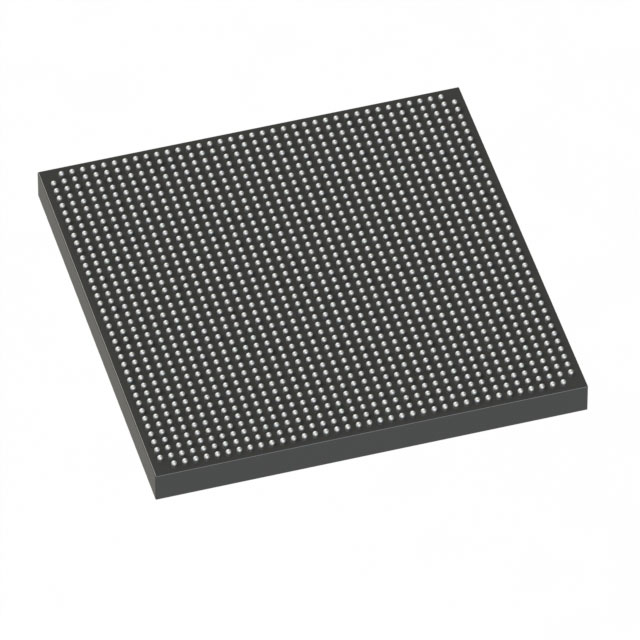
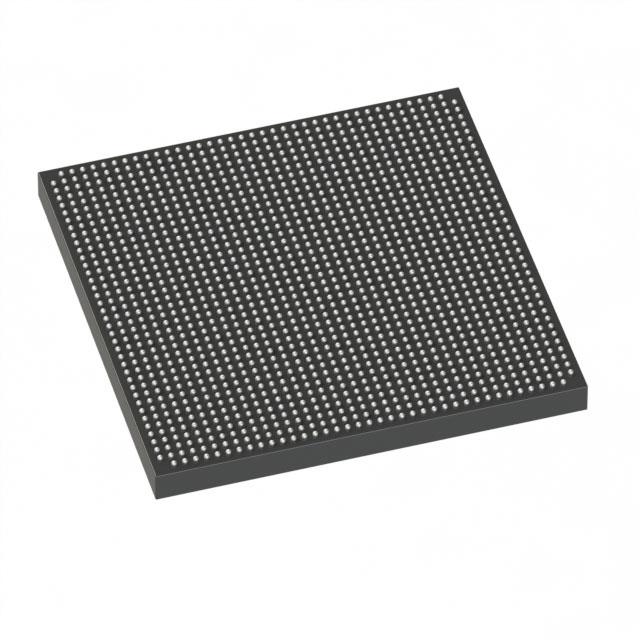
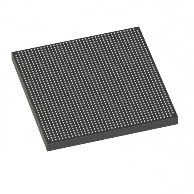
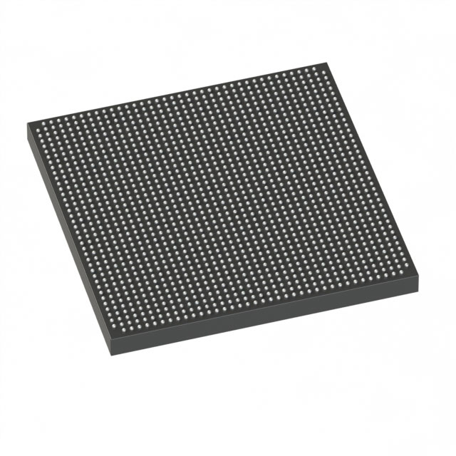
Key characteristics include 952,000 logic elements, approximately 53.25 Mbits of embedded RAM, and 696 user I/Os, packaged in a 1517-BBGA FCBGA (supplier package: 1517-HBGA, 45 × 45 mm) for surface-mount applications.
Key Features
- Logic Capacity — 952,000 logic elements provide a very large programmable fabric for complex digital signal processing, control, and custom logic implementations.
- Logic Blocks — Approximately 359,200 logic blocks (device topology) to structure large designs and partition functionality efficiently.
- Embedded Memory — Approximately 53.25 Mbits of on-chip RAM for frame buffers, FIFOs, and working memory to support data-intensive algorithms.
- I/O Resources — 696 user I/O pins to support dense external interfaces and multi‑channel connectivity.
- Package & Mounting — 1517-BBGA, FCBGA package (supplier device package: 1517-HBGA, 45 × 45 mm) designed for surface-mount PCB assembly.
- Power — Specified voltage supply range of 870 mV to 930 mV to define core supply requirements for power delivery design.
- Temperature & Grade — Commercial grade with an operating temperature range of 0 °C to 85 °C.
- Compliance — RoHS compliant.
- Family Transceiver Context — As a Stratix V GX device, the family supports defined transceiver speed grades in the datasheet for multi‑Gbps serial links (series-level specification).
Typical Applications
- High‑capacity FPGA designs — Use the large logic fabric and abundant embedded RAM for complex algorithm acceleration and data-path implementations.
- Multi‑I/O systems — Leverage 696 user I/Os for dense peripheral interfacing, board-level aggregation, and multi-channel connectivity.
- High‑speed serial systems — Deploy in systems that benefit from Stratix V GX family transceiver capabilities as specified at the series level in the device datasheet.
Unique Advantages
- Massive programmable capacity: 952,000 logic elements enable implementation of large-scale logic, DSP, and control functions without immediate partitioning across multiple devices.
- Substantial on‑chip memory: Approximately 53.25 Mbits of embedded RAM reduce external memory dependence for many buffering and streaming use cases.
- High I/O density: 696 I/Os simplify integration with multiple external subsystems and allow high channel counts on a single FPGA.
- Surface‑mount, compact package: 1517-BBGA / 1517-HBGA (45 × 45 mm) packaging provides a high‑pin‑count solution suitable for modern PCB assemblies.
- Commercial temperature grade: Specified 0 °C to 85 °C operating range aligns with a wide range of enterprise and embedded applications.
- RoHS compliant: Meets environmental compliance requirements for lead‑free designs.
Why Choose 5SGXMABK3H40C2NCV?
The 5SGXMABK3H40C2NCV delivers a high‑capacity Stratix V GX FPGA configuration targeted at designs that require deep logic resources, significant embedded memory, and extensive I/O in a commercial‑grade platform. Its package and pin count allow dense system integration while the documented core voltage range and operating temperature provide clear electrical and environmental boundaries for power‑delivery and thermal design.
This device is suited for teams developing large, performance‑oriented FPGA designs that need scalability within the Stratix V family and require the documented transceiver capabilities at the series level. Its combination of logic, memory, and I/O density helps reduce system-level component count and supports consolidated implementations on a single FPGA.
Request a quote or submit a product inquiry to check availability, pricing, and lead time for 5SGXMABK3H40C2NCV. Include your required quantities and any specific delivery or packaging needs to expedite the response.





















Date Founded: 1968
Headquarters: Santa Clara, California, USA
Employees: 130,000+
Revenue: $54.23 Billion
Certifications and Memberships: ISO9001:2015, ISO14001:2015, ISO17025:2017, ISO27001:2022, ISO45001:2018, ISO50001:2018


