
5SGXMB6R2F43I3LG
| Part Description |
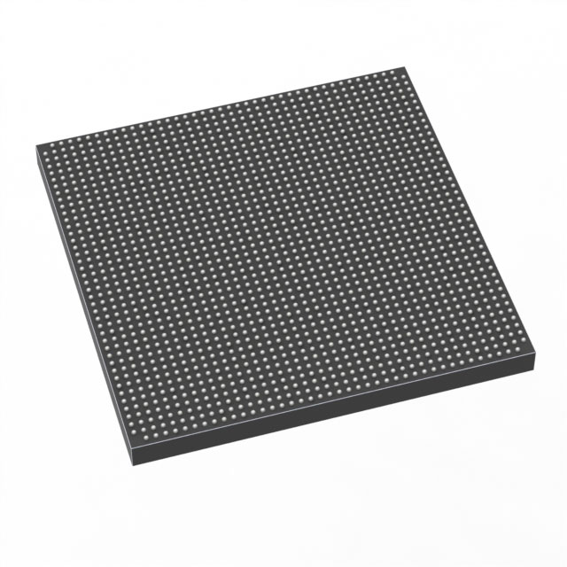
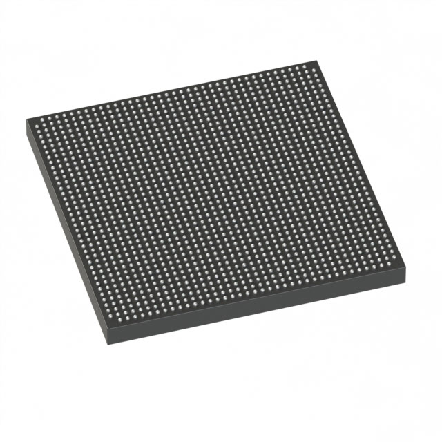
Stratix® V GX Field Programmable Gate Array (FPGA) IC 600 53248000 597000 1760-BBGA, FCBGA |
|---|---|
| Quantity | 25 Available (as of June 15, 2026) |

| Product Category | Field Programmable Gate Array (FPGA) |
|---|---|
| Manufacturer | Intel |
| Manufacturing Status | Active |
| Manufacturer Standard Lead Time | 26 Weeks |
| Datasheet |
Specifications & Environmental
| Device Package | 1760-FCBGA (42.5x42.5) | Grade | Industrial | Operating Temperature | -40°C – 100°C | ||
|---|---|---|---|---|---|---|---|
| Package / Case | 1760-BBGA, FCBGA | Number of I/O | 600 | Voltage | 820 mV - 880 mV | ||
| Mounting Method | Surface Mount | RoHS Compliance | RoHS Compliant | REACH Compliance | REACH Unaffected | ||
| Moisture Sensitivity Level | 3 (168 Hours) | Number of LABs/CLBs | 225400 | Number of Logic Elements/Cells | 597000 | ||
| Number of Gates | N/A | ECCN | N/A | HTS Code | N/A | ||
| Qualification | N/A | Total RAM Bits | 53248000 |
Overview of 5SGXMB6R2F43I3LG – Stratix® V GX FPGA IC, 597,000 logic elements, approximately 53.25 Mbits RAM, 600 I/Os, 1760-FCBGA
The Intel Stratix® V GX Field Programmable Gate Array (FPGA) 5SGXMB6R2F43I3LG is an industrial-grade, high-density programmable logic device in a 1760-FCBGA (42.5 × 42.5 mm) package. It delivers large on-chip logic and embedded memory capacity alongside a high I/O count, making it appropriate for complex, I/O-rich designs that require significant programmable logic and memory resources.
As a member of the Stratix V GX family, the device is part of a series documented for its electrical and switching characteristics, including transceiver capability and core/periphery performance as described in the Stratix V device datasheet.
Key Features
- Core logic density — 597,000 logic elements providing substantial programmable logic capacity for complex designs.
- Logic block count — 225,400 logic blocks available for partitioning and architectural flexibility within designs.
- Embedded memory — approximately 53.25 Mbits of on-chip RAM for buffering, state storage, and data-path implementations.
- High I/O count — 600 user I/Os to support wide parallel interfaces and multiple peripherals.
- Package and mounting — 1760-FCBGA (42.5 × 42.5 mm) surface-mount package for high-pin-count board integration.
- Voltage supply — core voltage range of 820 mV to 880 mV to align with modern FPGA core power domains.
- Industrial operating range — rated for operation from −40 °C to 100 °C for deployment in industrial environments.
- Standards compliance — RoHS compliant.
- Family-level transceiver capability — Stratix V GX family documentation lists transceiver speed grades (family-level information includes options up to 14.1 Gbps as shown in the device datasheet).
Typical Applications
- High-density programmable logic systems — for designs that require hundreds of thousands of logic elements to implement complex state machines, custom datapaths, and large combinational/sequential logic blocks.
- Memory-centric designs — where tens of megabits of on-chip RAM reduce external memory dependence for buffering, FIFOs, or lookup tables.
- I/O-intensive systems — boards or modules requiring large parallel or multiplexed interfaces supported by 600 available I/Os.
Unique Advantages
- Substantial programmable capacity: 597,000 logic elements enable large, highly integrated FPGA designs without splitting functions across multiple devices.
- Significant embedded memory: approximately 53.25 Mbits of on-chip RAM reduces external memory needs and simplifies board-level design.
- High I/O availability: 600 I/Os support complex multi-interface systems and parallel data paths.
- Industrial temperature rating: specified operation from −40 °C to 100 °C for use in industrial operating environments.
- High-pin-count FCBGA package: 1760-FCBGA (42.5 × 42.5 mm) provides a compact footprint for integrating a large number of signals on complex PCBs.
- Family-level performance documentation: Stratix V device datasheet provides electrical, switching, and transceiver characteristic details to guide system integration.
Why Choose 5SGXMB6R2F43I3LG?
The 5SGXMB6R2F43I3LG offers a combination of high logic density, substantial on-chip memory, and a large I/O count in an industrial-grade Stratix V GX device package. This combination is tailored for engineers developing complex, I/O-heavy systems that need substantial programmable resources while operating across a wide industrial temperature range.
Designed as part of the Stratix V family, the device is supported by detailed electrical and switching characteristic documentation, allowing engineering teams to evaluate core, periphery, and transceiver behavior during system design and integration.
Request a quote or submit an inquiry to receive pricing and lead-time information for the 5SGXMB6R2F43I3LG Stratix V GX FPGA.


Date Founded: 1968
Headquarters: Santa Clara, California, USA
Employees: 130,000+
Revenue: $54.23 Billion
Certifications and Memberships: ISO9001:2015, ISO14001:2015, ISO17025:2017, ISO27001:2022, ISO45001:2018, ISO50001:2018


