
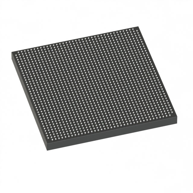
5SGXMB6R3F40I3LG
| Part Description |
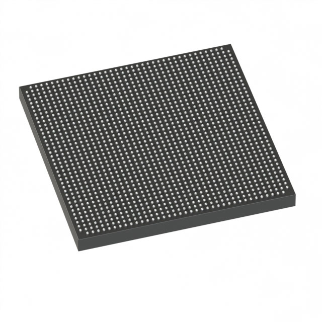
Stratix® V GX Field Programmable Gate Array (FPGA) IC 432 53248000 597000 1517-FBGA (40x40) |
|---|---|
| Quantity | 1,560 Available (as of October 8, 2026) |
| Product Category | Field Programmable Gate Array (FPGA) |
|---|---|
| Manufacturer | Intel |
| Manufacturing Status | Active |
| Manufacturer Standard Lead Time | 26 Weeks |
| Datasheet |
Specifications & Environmental
| Device Package | 1517-FBGA (40x40) | Grade | Industrial | Operating Temperature | -40°C – 100°C | ||
|---|---|---|---|---|---|---|---|
| Package / Case | 1517-FBGA (40x40) | Number of I/O | 432 | Voltage | 820 mV - 880 mV | ||
| Mounting Method | Surface Mount | RoHS Compliance | RoHS Compliant | REACH Compliance | REACH Unaffected | ||
| Moisture Sensitivity Level | 3 (168 Hours) | Number of LABs/CLBs | 225400 | Number of Logic Elements/Cells | 597000 | ||
| Number of Gates | N/A | ECCN | N/A | HTS Code | N/A | ||
| Qualification | N/A | Total RAM Bits | 53248000 |
Overview of 5SGXMB6R3F40I3LG – Stratix V GX FPGA IC, 1517-FBGA (40×40)
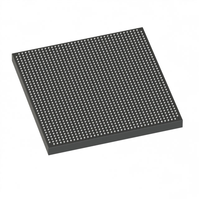
The 5SGXMB6R3F40I3LG is a Stratix® V GX field programmable gate array (FPGA) IC from Intel, supplied in a 1517‑ball FBGA (40×40) package. It delivers very high logic capacity and embedded memory combined with a large I/O count, making it suitable for dense digital processing and systems that require substantial on‑chip resources.
This device targets applications requiring extensive programmable logic (597,000 logic elements), approximately 53.25 Mbits of embedded RAM, and up to 432 user I/O while supporting industrial temperature operation and low‑voltage core operation.
Key Features
- Core Logic 597,000 logic elements provide substantial programmable fabric for complex logic, DSP, and custom accelerator implementations.
- Logic Array Blocks (LABs) 225,400 LABs for organized, high-density logic placement and routing.
- Embedded Memory Approximately 53.25 Mbits of on-chip RAM to support large buffers, FIFOs, and memory-intensive algorithms without external memory dependency.
- High I/O Count Up to 432 user I/O pins to accommodate multi-channel interfaces and dense board-level connectivity.
- Package and Mounting 1517‑FBGA (40×40) package with surface-mount mounting type for compact system integration.
- Power and Operating Conditions Core supply range of 820 mV to 880 mV and rated for industrial operating temperatures from −40 °C to 100 °C.
- Regulatory Status RoHS compliant.
Typical Applications
- High‑density signal processing — Large logic capacity and substantial embedded RAM enable implementation of complex DSP pipelines and packet processing engines.
- Multi‑channel I/O systems — 432 I/Os support boards that require many parallel interfaces or dense sensor/actuator connectivity.
- Industrial control and automation — Industrial temperature grade and wide operating voltage compatibility suit rugged embedded systems.
- Custom accelerators and coprocessors — High logic and memory resources make this device well matched for hardware acceleration blocks and offload engines.
Unique Advantages
- Very high programmable capacity: 597,000 logic elements enable implementation of large, complex designs on a single device, reducing system-level component count.
- Substantial on‑chip memory: Approximately 53.25 Mbits of embedded RAM reduce reliance on external memory and simplify board layout and BOM.
- Extensive I/O capability: 432 I/Os allow flexible connectivity for multi‑lane interfaces, parallel buses, and mixed-signal front ends.
- Industrial temperature rating: −40 °C to 100 °C operation supports deployment in demanding environmental conditions.
- Compact BGA packaging: 1517‑FBGA (40×40) balances high pin count with a compact footprint for space-constrained designs.
- Low‑voltage core operation: 820–880 mV supply range aligns with modern low-power FPGA core requirements.
Why Choose 5SGXMB6R3F40I3LG?
The 5SGXMB6R3F40I3LG is positioned for designs that demand large-scale programmable logic, significant embedded memory, and wide I/O capability within an industrial temperature envelope. Its combination of nearly 600k logic elements, substantial on‑chip RAM, and high I/O count provides designers with the resources needed to consolidate functionality and reduce overall system complexity.
As part of the Stratix V GX family and supported by the Stratix V device documentation, this device is suitable for engineers building high-performance, memory‑intensive, and connectivity‑rich solutions that require robust temperature and voltage operation.
Request a quote or submit an RFQ to obtain pricing and availability for part number 5SGXMB6R3F40I3LG.





















Date Founded: 1968
Headquarters: Santa Clara, California, USA
Employees: 130,000+
Revenue: $54.23 Billion
Certifications and Memberships: ISO9001:2015, ISO14001:2015, ISO17025:2017, ISO27001:2022, ISO45001:2018, ISO50001:2018


