
5SGXMBBR1H43C2G
| Part Description |
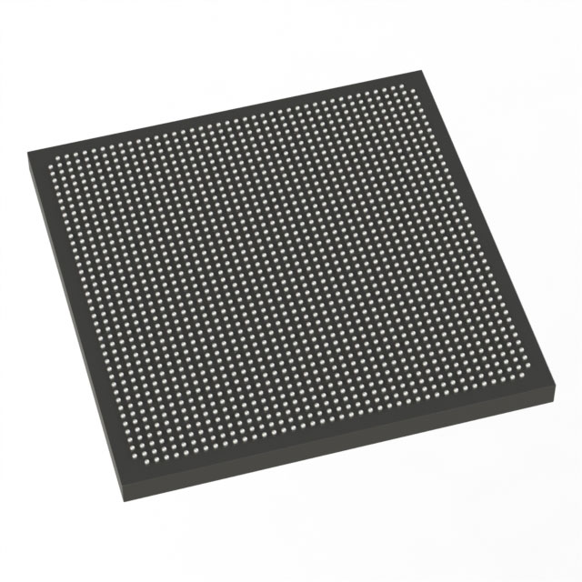
Stratix® V GX Field Programmable Gate Array (FPGA) IC 600 53248000 952000 1760-BBGA, FCBGA |
|---|---|
| Quantity | 355 Available (as of June 10, 2026) |

| Product Category | Field Programmable Gate Array (FPGA) |
|---|---|
| Manufacturer | Intel |
| Manufacturing Status | Active |
| Manufacturer Standard Lead Time | 26 Weeks |
| Datasheet |
Specifications & Environmental
| Device Package | 1760-HBGA (45x45) | Grade | Commercial | Operating Temperature | 0°C – 85°C | ||
|---|---|---|---|---|---|---|---|
| Package / Case | 1760-BBGA, FCBGA | Number of I/O | 600 | Voltage | 870 mV - 930 mV | ||
| Mounting Method | Surface Mount | RoHS Compliance | RoHS Compliant | REACH Compliance | REACH Unaffected | ||
| Moisture Sensitivity Level | 3 (168 Hours) | Number of LABs/CLBs | 359200 | Number of Logic Elements/Cells | 952000 | ||
| Number of Gates | N/A | ECCN | N/A | HTS Code | N/A | ||
| Qualification | N/A | Total RAM Bits | 53248000 |
Overview of 5SGXMBBR1H43C2G – Stratix® V GX Field Programmable Gate Array (FPGA) IC
The 5SGXMBBR1H43C2G is a Stratix V GX family FPGA from Intel, delivering very large programmable logic capacity, abundant on-chip memory, and extensive I/O in a high-pin-count FCBGA package. It is intended for commercial applications that require consolidation of complex digital functions into a single, high-density FPGA.
Engineered for designs that need large logic arrays, significant embedded RAM, and broad external connectivity, this device pairs the Stratix V GX architecture with the datasheet-backed electrical and switching characteristics provided by Intel/Altera documentation.
Key Features
- Core Logic Capacity — 952,000 logic elements and 359,200 CLBs provide high-density programmable logic for complex designs.
- Embedded Memory — Approximately 53.25 Mbits of on-chip RAM for buffering, data storage, and memory-intensive functions.
- I/O Density — 600 user I/O pins to support dense peripheral and board-level connectivity.
- Package & Mounting — 1760-BBGA, FCBGA package (supplier device package: 1760-HBGA, 45×45); surface-mount construction for compact, high-pin-count implementations.
- Power — Core voltage supply range: 870 mV to 930 mV, enabling defined power budgeting and supply design.
- Temperature & Grade — Commercial grade device with an operating temperature range of 0°C to 85°C.
- Regulatory — RoHS compliant.
- Series Documentation — Part of the Stratix V GX family; documented electrical and switching characteristics are available in the Stratix V device datasheet.
Typical Applications
- High-density logic implementations — Consolidate complex digital functions using the device's 952,000 logic elements to reduce board-level component count.
- Memory-intensive processing — Approximately 53.25 Mbits of embedded RAM supports on-chip buffering and intermediate data storage for data-path and signal-processing tasks.
- I/O-rich systems — 600 I/Os enable integration with multiple peripherals, sensors, or daughter cards in communication and interface-heavy designs.
- Designs leveraging Stratix V GX transceiver options — Use alongside the Stratix V device documentation to exploit available transceiver and I/O timing capabilities for high-speed link implementations.
Unique Advantages
- High logic density: 952,000 logic elements let you implement large, integrated designs on a single device, reducing BOM complexity.
- Substantial on-chip memory: Approximately 53.25 Mbits of embedded RAM lowers dependence on external memory and improves data locality.
- Extensive external connectivity: 600 user I/Os provide the flexibility needed for complex board-level integration and multiple interface standards.
- Commercial-grade operating range: Rated 0°C to 85°C for use in standard commercial environments.
- Compact, high-pin-count package: 1760-BBGA / 1760-HBGA (45×45) surface-mount package balances pin density and board footprint.
- RoHS compliant: Supports lead-free manufacturing and regulatory requirements.
Why Choose 5SGXMBBR1H43C2G?
The 5SGXMBBR1H43C2G positions itself as a high-capacity, commercially graded Stratix V GX FPGA for designs that demand large programmable logic resources, significant embedded RAM, and a high I/O count. Its specified core voltage range and package options support system-level integration where power budgeting and board layout must be carefully managed.
This device is suited to engineering teams and procurement groups targeting consolidation of complex logic and memory functions into a single FPGA, with specification-level documentation available through the Stratix V device datasheet to support electrical, timing, and transceiver design decisions.
Request a quote or submit a request for pricing and availability to obtain product lead time, pricing, and ordering information for 5SGXMBBR1H43C2G.


Date Founded: 1968
Headquarters: Santa Clara, California, USA
Employees: 130,000+
Revenue: $54.23 Billion
Certifications and Memberships: ISO9001:2015, ISO14001:2015, ISO17025:2017, ISO27001:2022, ISO45001:2018, ISO50001:2018


