
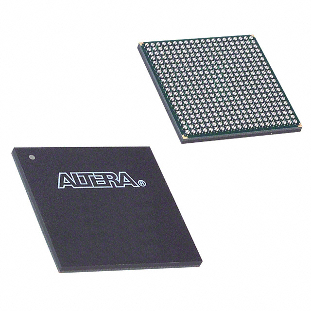
EP1C20F400C8
| Part Description |
Cyclone® Field Programmable Gate Array (FPGA) IC 301 294912 20060 400-BGA |
|---|---|
| Quantity | 257 Available (as of June 15, 2026) |

| Product Category | Field Programmable Gate Array (FPGA) |
|---|---|
| Manufacturer | Intel |
| Manufacturing Status | Obsolete |
| Manufacturer Standard Lead Time | Contact Us |
| Datasheet |
Specifications & Environmental
| Device Package | 400-FBGA (21x21) | Grade | Commercial | Operating Temperature | 0°C – 85°C | ||
|---|---|---|---|---|---|---|---|
| Package / Case | 400-BGA | Number of I/O | 301 | Voltage | 1.425 V - 1.575 V | ||
| Mounting Method | Surface Mount | RoHS Compliance | RoHS non-compliant | REACH Compliance | REACH Unknown | ||
| Moisture Sensitivity Level | 3 (168 Hours) | Number of LABs/CLBs | 2006 | Number of Logic Elements/Cells | 20060 | ||
| Number of Gates | N/A | ECCN | 3A991D | HTS Code | 8542.39.0001 | ||
| Qualification | N/A | Total RAM Bits | 294912 |
Overview of EP1C20F400C8 – Cyclone FPGA, 20,060 logic elements, 294,912 bits RAM, 400‑BGA
The EP1C20F400C8 is a Cyclone® field programmable gate array supplied in a 400‑ball BGA package. It delivers a mid‑range FPGA fabric with 20,060 logic elements, substantial on‑chip RAM, and up to 301 user I/O pins, making it suitable for cost‑sensitive data‑path and control applications.
Built on the Cyclone family architecture, the device combines SRAM‑based logic, on‑chip memory blocks, and clocking resources to support a variety of embedded logic, interface bridging, and I/O‑intensive designs within a commercial temperature range.
Key Features
- Logic Capacity — 20,060 logic elements (LEs) provide flexible fabric for combinational and sequential logic implementation.
- On‑chip Memory — 294,912 total RAM bits of embedded memory to implement FIFOs, buffers, and small local memories.
- I/O Density — Up to 301 user I/O pins support broad peripheral and system interfacing needs.
- Clocking — Family features include up to two PLLs and multiple global clock resources to enable clock multiplication and phase alignment for synchronous systems.
- Process and Power — Device family is based on a 1.5‑V, 0.13‑µm, all‑layer copper SRAM process; this part’s specified core supply range is 1.425 V to 1.575 V.
- Package and Mounting — Surface‑mount 400‑ball BGA (400‑FBGA, 21 × 21) for compact board integration and thermal distribution.
- Temperature and Grade — Commercial grade operation with an ambient operating temperature range of 0 °C to 85 °C.
- Family I/O Support — Cyclone family-level support for multiple I/O standards and high‑speed interfaces, including LVDS and DDR memory interfaces (as defined by the Cyclone device family).
- RoHS Compliance — Device is RoHS compliant.
Typical Applications
- Protocol and Interface Bridging — Implement protocol translation and custom interface logic where a mix of high I/O count and embedded memory is required.
- Data Path Acceleration — Use on‑chip RAM and programmable logic for packet buffering, simple DSP blocks, and timing‑sensitive data flows.
- Embedded Control and Glue Logic — Replace multiple discrete components by consolidating state machines, bus controllers, and peripheral logic in a single FPGA fabric.
- Prototype and Product Development — Applicable for commercial‑temperature prototypes and production designs that require reprogrammable hardware for iterative development or field updates.
Unique Advantages
- High Logic Density: 20,060 logic elements enable complex logic consolidation while keeping board footprint compact.
- Substantial Embedded Memory: 294,912 bits of on‑chip RAM reduce external memory dependence for many buffering and small‑memory use cases.
- Generous I/O Count: Up to 301 I/O pins allow direct connection to multiple buses, peripherals, and external devices without intermediate multiplexing.
- Flexible Clocking Resources: On‑device PLLs and global clock lines support diverse timing architectures and synchronous domain management.
- Compact BGA Package: 400‑FBGA (21 × 21) minimizes PCB area while providing reliable solder connectivity for surface‑mount assembly.
- Commercial Temperature Suitability: Rated for 0 °C to 85 °C, suitable for a wide range of non‑industrial, non‑automotive applications.
Why Choose EP1C20F400C8?
The EP1C20F400C8 positions itself as a practical choice for designers needing mid‑range FPGA capacity with ample embedded memory and high I/O connectivity in a compact BGA footprint. Its Cyclone family heritage brings familiar architecture and family‑level features—such as PLLs and support for common high‑speed I/O standards—into designs that benefit from reprogrammable logic and in‑system flexibility.
This device suits teams developing commercial‑temperature products that require integration of control logic, interface bridging, or data‑path buffering while keeping board space and component count under control. Its combination of logic elements, on‑chip RAM, and pin‑count offers a balanced platform for both prototype and production deployments backed by Cyclone family documentation and tooling.
Request a quote or submit a procurement inquiry to obtain pricing, lead time, and availability for EP1C20F400C8.


Date Founded: 1968
Headquarters: Santa Clara, California, USA
Employees: 130,000+
Revenue: $54.23 Billion
Certifications and Memberships: ISO9001:2015, ISO14001:2015, ISO17025:2017, ISO27001:2022, ISO45001:2018, ISO50001:2018


