
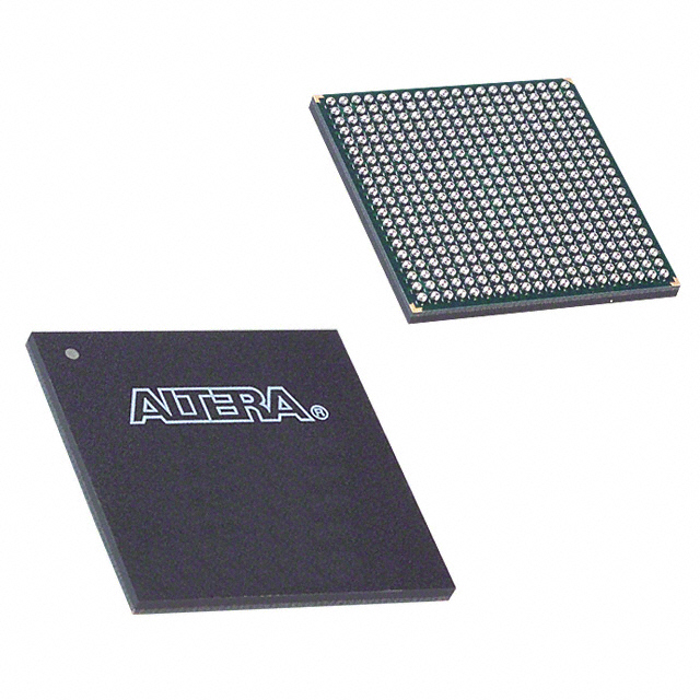
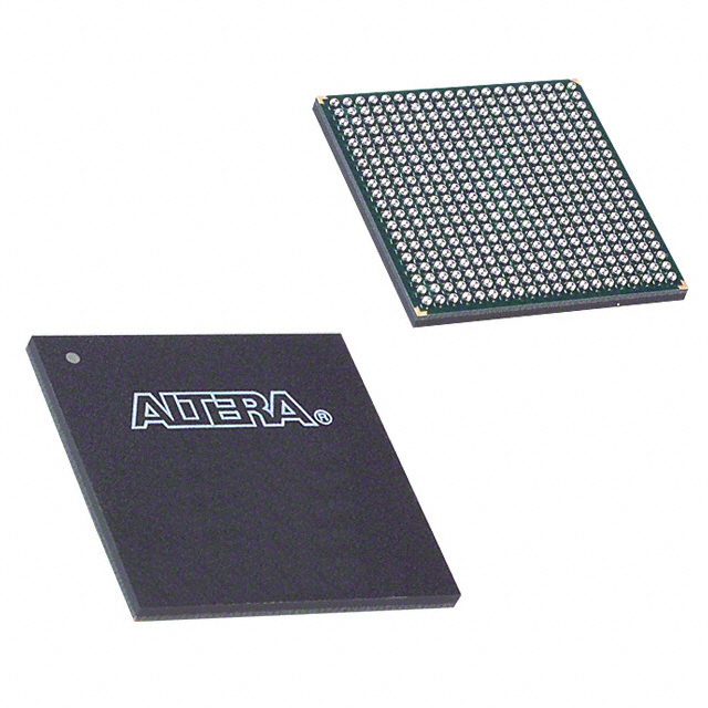
EP1C20F400C7N
| Part Description |
Cyclone® Field Programmable Gate Array (FPGA) IC 301 294912 20060 400-BGA |
|---|---|
| Quantity | 664 Available (as of October 8, 2026) |
| Product Category | Field Programmable Gate Array (FPGA) |
|---|---|
| Manufacturer | Intel |
| Manufacturing Status | Obsolete |
| Manufacturer Standard Lead Time | Contact Us |
| Datasheet |
Specifications & Environmental
| Device Package | 400-FBGA (21x21) | Grade | Commercial | Operating Temperature | 0°C – 85°C | ||
|---|---|---|---|---|---|---|---|
| Package / Case | 400-BGA | Number of I/O | 301 | Voltage | 1.425 V - 1.575 V | ||
| Mounting Method | Surface Mount | RoHS Compliance | Unknown | REACH Compliance | REACH Unknown | ||
| Moisture Sensitivity Level | 3 (168 Hours) | Number of LABs/CLBs | 2006 | Number of Logic Elements/Cells | 20060 | ||
| Number of Gates | N/A | ECCN | 3A991D | HTS Code | 8542.39.0001 | ||
| Qualification | N/A | Total RAM Bits | 294912 |
Overview of EP1C20F400C7N – Cyclone® Field Programmable Gate Array (FPGA) IC 301 294912 20060 400-BGA
The EP1C20F400C7N is a Cyclone® family Field Programmable Gate Array (FPGA) from Intel designed for cost-effective data-path and interface applications. It combines a high logic capacity with substantial on-chip memory and extensive I/O to support embedded systems, communications equipment, and custom peripheral interfaces.
Key architectural attributes include up to 20,060 logic elements, approximately 0.295 Mbits of embedded RAM, support for multiple I/O standards and high-speed LVDS, and up to two PLLs for flexible clocking. The device ships in a 400-ball BGA (400-FBGA, 21×21) surface-mount package and is specified for commercial-grade operation.
Key Features
- Core Capacity Up to 20,060 logic elements provide dense programmable logic for complex combinational and sequential designs.
- Embedded Memory Approximately 0.295 Mbits (294,912 bits) of on-chip RAM for data buffering, FIFOs, and small embedded memory structures.
- I/O Count & Standards 301 user I/O pins and support for LVTTL, LVCMOS, SSTL-2, SSTL-3 I/O standards enable broad system interfacing options.
- High-speed Serial and Parallel I/O Supports high-speed LVDS (up to 640 Mbps) and RSDS (311 Mbps) interfaces; supports 66- and 33-MHz, 64- and 32-bit PCI signaling for peripheral connectivity.
- Clocking Resources Up to two PLLs per device with multiple global clock resources to implement clock multiplication and phase shifting for complex timing domains.
- Memory and External Interfaces Architecture supports external memory interfaces including DDR SDRAM, FCRAM, and SDR SDRAM for systems requiring expanded external storage.
- Package & Mounting 400-ball FineLine BGA (400-FBGA, 21×21) surface-mount package balances pin count and board-area efficiency for compact systems.
- Power & Operating Range Voltage supply range from 1.425 V to 1.575 V and commercial operating temperature from 0 °C to 85 °C.
- Compliance RoHS compliant for lead-free manufacturing environments.
Typical Applications
- Data-path Processing Use the device’s large logic density and embedded RAM to implement packet processing, stream alignment, and custom datapath pipelines.
- Memory Interface and Buffering Implement DDR SDRAM or SDRAM controllers and local buffering utilizing the device’s on-chip RAM and external-memory support.
- High-speed I/O Bridging Leverage 301 I/Os and LVDS support to realize high-speed board-level interfaces, SERDES-less data links, and parallel-to-serial bridging.
- Custom Peripheral and Bus Logic Implement PCI-compatible interfaces, glue logic, and custom peripheral controllers that require flexible I/O standards and abundant logic resources.
Unique Advantages
- High Logic Density: With up to 20,060 logic elements, the device supports complex RTL implementations without external glue logic.
- Substantial On-chip Memory: Approximately 0.295 Mbits of embedded RAM reduces reliance on external memory for small buffers and state storage.
- Flexible I/O and Signaling: 301 I/O pins and support for multiple I/O standards, LVDS, and PCI signaling simplify integration with a wide range of peripherals and boards.
- Integrated Clocking: Dual PLLs and multiple global clock resources enable robust multi-domain clock architectures and timing adjustments on-chip.
- Compact Surface-mount Package: The 400-FBGA (21×21) package provides high pin density in a compact footprint for space-constrained PCBs.
- Design Migration and Tool Support: Cyclone family features facilitate device migration across densities and are supported by vendor design flows and IP cores documented in the device handbook.
Why Choose EP1C20F400C7N?
The EP1C20F400C7N positions itself as a commercially graded Cyclone FPGA that blends significant logic capacity, compact packaging, and versatile I/O to address demanding data-path and interface roles. Its combination of approximately 20k logic elements, nearly 0.295 Mbits of embedded RAM, high I/O count, and support for modern I/O standards makes it suitable for embedded systems and communications equipment where integration and configurable hardware matter.
Chosen for designs that need scalability and practical vendor-supported IP and toolchains, this device offers a balance of performance, integration, and manufacturability for commercial-grade applications where programmable logic enables custom hardware differentiation.
Request a quote or submit availability and pricing requests to receive lead-time and purchasing details for EP1C20F400C7N.




















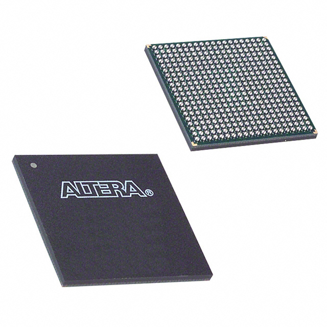
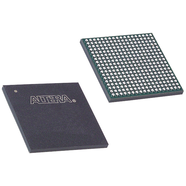


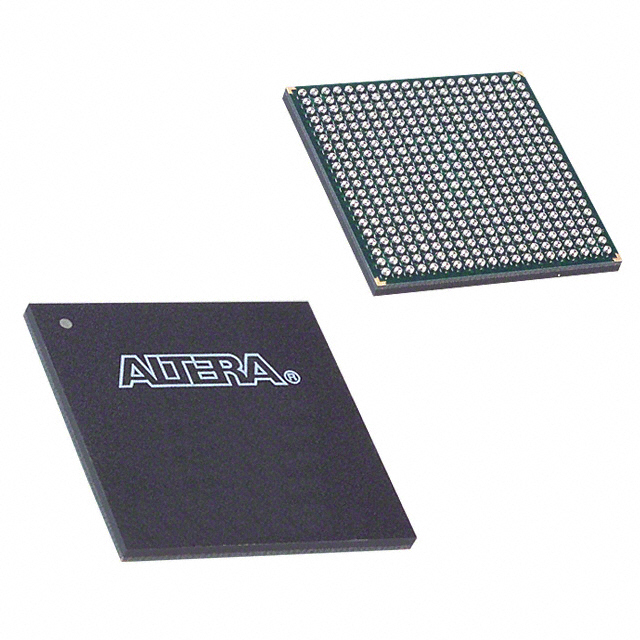



Date Founded: 1968
Headquarters: Santa Clara, California, USA
Employees: 130,000+
Revenue: $54.23 Billion
Certifications and Memberships: ISO9001:2015, ISO14001:2015, ISO17025:2017, ISO27001:2022, ISO45001:2018, ISO50001:2018


