
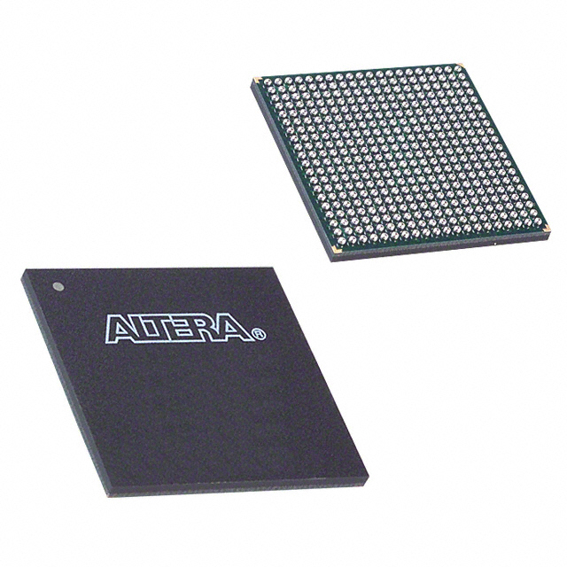
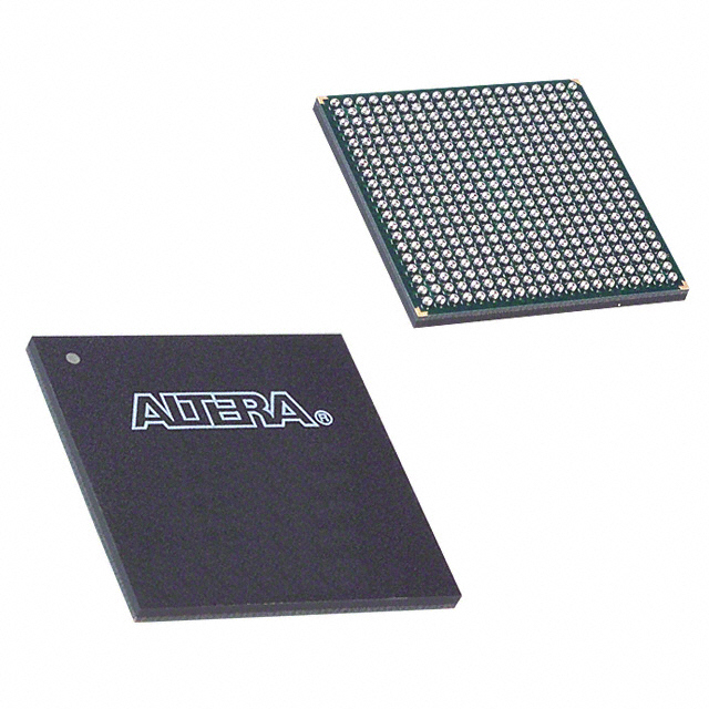
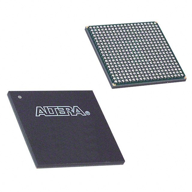
EP1C20F400C8N
| Part Description |
Cyclone® Field Programmable Gate Array (FPGA) IC 301 294912 20060 400-BGA |
|---|---|
| Quantity | 828 Available (as of October 8, 2026) |

| Product Category | Field Programmable Gate Array (FPGA) |
|---|---|
| Manufacturer | Intel |
| Manufacturing Status | Obsolete |
| Manufacturer Standard Lead Time | Contact Us |
| Datasheet |
Specifications & Environmental
| Device Package | 400-FBGA (21x21) | Grade | Commercial | Operating Temperature | 0°C – 85°C | ||
|---|---|---|---|---|---|---|---|
| Package / Case | 400-BGA | Number of I/O | 301 | Voltage | 1.425 V - 1.575 V | ||
| Mounting Method | Surface Mount | RoHS Compliance | Unknown | REACH Compliance | REACH Unknown | ||
| Moisture Sensitivity Level | 3 (168 Hours) | Number of LABs/CLBs | 2006 | Number of Logic Elements/Cells | 20060 | ||
| Number of Gates | N/A | ECCN | 3A991D | HTS Code | 8542.39.0001 | ||
| Qualification | N/A | Total RAM Bits | 294912 |
Overview of EP1C20F400C8N – Cyclone Field Programmable Gate Array, 20,060 logic elements, 400‑BGA
The EP1C20F400C8N is a Cyclone® series Field Programmable Gate Array (FPGA) optimized for data-path and interface-centric applications. It delivers 20,060 logic elements in a compact 400‑FBGA (21×21) surface‑mount package, making it suitable for designs that require significant logic capacity and flexible I/O in a space-constrained board footprint.
Built on the Cyclone device architecture, this device offers integrated on-chip memory, multiple clocking resources, and broad I/O capability—features aimed at communications, embedded control, and memory‑interface designs where integration and predictable supply and thermal ranges are important.
Key Features
- Core Logic 20,060 logic elements provide substantial programmable fabric for combinational and sequential logic functions.
- Embedded Memory Approximately 0.295 Mbits of on-chip RAM (294,912 bits) for FIFOs, buffers, and small on-chip data stores.
- I/O and Interface Support Up to 301 user I/O pins enable wide peripheral and bus connectivity; Cyclone series devices support LVTTL, LVCMOS, SSTL‑2/SSTL‑3 and high‑speed LVDS signaling as documented for the device family.
- Clocking and Timing Up to two PLLs per device and multiple global clock resources support clock multiplication, phase shifting, and flexible clock distribution within the device.
- Package and Mounting 400‑FBGA (21×21) package in a surface‑mount form factor for compact board layouts and high I/O density.
- Power and Operating Range Supported core supply range of 1.425 V to 1.575 V with a commercial operating temperature range of 0 °C to 85 °C.
- Standards and Ecosystem Device family documentation notes support for common memory interfaces (DDR SDRAM, SDR SDRAM, FCRAM) and integration with Altera/Quartus® II development tools and megafunction/IP offerings for faster design implementation.
- Regulatory RoHS compliant.
Typical Applications
- High‑throughput data paths — Use the EP1C20F400C8N for packet processing, data aggregation, or protocol translation where dense logic and on‑chip RAM accelerate real‑time processing.
- Memory interface controllers — Implement DDR SDRAM and SDRAM controller logic leveraging the device family’s documented external memory support and available PLL resources.
- Serial and parallel I/O bridging — Ideal for bridging between high‑speed LVDS links and parallel host buses or ASSP/ASIC interfaces using the device’s extensive I/O count and supported signaling standards.
- Embedded system glue logic — Integrate custom peripherals, user interfaces, and control logic into a single FPGA to reduce BOM and simplify board-level routing.
Unique Advantages
- High logic density: 20,060 logic elements enable complex designs and multi‑function integration without partitioning across multiple devices.
- Meaningful on‑chip RAM: Approximately 0.295 Mbits of embedded memory reduces dependence on external RAM for small buffers and state storage.
- Wide I/O capability: 301 user I/O pins support extensive peripheral and bus connectivity, enabling flexible system interfaces.
- Compact BGA footprint: 400‑FBGA (21×21) delivers high I/O in a compact surface‑mount package suitable for space‑constrained designs.
- Commercial temperature rating: Specified for 0 °C to 85 °C operation to match mainstream embedded and consumer electronics requirements.
- Toolchain and IP compatibility: Family documentation indicates compatibility with Quartus® II tools and Altera megafunction/IP options to accelerate development and migration.
Why Choose EP1C20F400C8N?
The EP1C20F400C8N positions itself as a balanced FPGA option where substantial logic resources, usable on‑chip memory, and extensive I/O converge in a compact BGA package. Its documented family features—clocking resources, memory interface support, and IP integration—help shorten development time for data‑path, memory controller, and interface bridging applications.
This device is well suited to engineers and teams building embedded systems, communications interfaces, or custom hardware accelerators who need a commercially graded FPGA with predictable supply and thermal parameters, and access to the Cyclone device toolchain and megafunction library for faster deployment.
Request a quote or submit an inquiry to purchase EP1C20F400C8N and evaluate how this Cyclone FPGA can streamline your next design.

























Date Founded: 1968
Headquarters: Santa Clara, California, USA
Employees: 130,000+
Revenue: $54.23 Billion
Certifications and Memberships: ISO9001:2015, ISO14001:2015, ISO17025:2017, ISO27001:2022, ISO45001:2018, ISO50001:2018


