
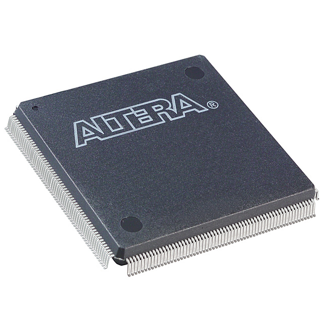
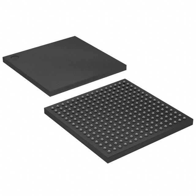
EP1C6F256C8N
| Part Description |
Cyclone® Field Programmable Gate Array (FPGA) IC 185 92160 5980 256-BGA |
|---|---|
| Quantity | 680 Available (as of June 10, 2026) |

| Product Category | Field Programmable Gate Array (FPGA) |
|---|---|
| Manufacturer | Intel |
| Manufacturing Status | Obsolete |
| Manufacturer Standard Lead Time | Contact Us |
| Datasheet |
Specifications & Environmental
| Device Package | 256-FBGA (17x17) | Grade | Commercial | Operating Temperature | 0°C – 85°C | ||
|---|---|---|---|---|---|---|---|
| Package / Case | 256-BGA | Number of I/O | 185 | Voltage | 1.425 V - 1.575 V | ||
| Mounting Method | Surface Mount | RoHS Compliance | Unknown | REACH Compliance | REACH Unknown | ||
| Moisture Sensitivity Level | 3 (168 Hours) | Number of LABs/CLBs | 598 | Number of Logic Elements/Cells | 5980 | ||
| Number of Gates | N/A | ECCN | 3A991D | HTS Code | 8542.39.0001 | ||
| Qualification | N/A | Total RAM Bits | 92160 |
Overview of EP1C6F256C8N – Cyclone® FPGA IC, 5,980 Logic Elements, 256‑BGA
The EP1C6F256C8N is an Intel Cyclone® field programmable gate array offering mid-range logic capacity and on-chip RAM for data-path and interface applications. Built for commercial-grade deployments, this device combines approximately 5,980 logic elements with 92,160 bits of embedded RAM and up to 185 user I/O pins to support moderate-density programmable logic designs.
This Cyclone device targets designers who need efficient integration of logic, memory, and flexible I/O in a compact 256‑FBGA (17×17) surface-mount package, with low-voltage operation and standard commercial temperature range support.
Key Features
- Logic Capacity Approximately 5,980 logic elements suitable for mid-density integration of custom logic and control functions.
- Embedded Memory 92,160 total on-chip RAM bits (approximately 0.09 Mbits) for buffering, FIFOs, and small data structures.
- I/O Density and Standards Up to 185 user I/O pins to accommodate wide parallel interfaces; series documentation indicates support for common I/O standards including LVTTL, LVCMOS, SSTL, and LVDS.
- Clocking Resources Device-level documentation specifies up to two PLLs for clock multiplication and phase shifting to support complex timing requirements.
- Package and Mounting 256‑FBGA (17×17) package in a surface-mount format for compact board designs and high pin density.
- Power Core supply range of 1.425 V to 1.575 V for low-voltage operation.
- Operating Range and Grade Commercial grade operation with an operating temperature range of 0 °C to 85 °C.
- Compliance RoHS compliant to meet regulatory requirements for lead-free assembly.
Typical Applications
- Data-Path Processing: Use the device’s logic elements and on-chip RAM to implement packet processing, data formatting, and custom arithmetic pipelines in mid-density systems.
- Memory Interface Bridging: Integrate with external DDR SDRAM or FCRAM interfaces using the device’s clocking resources and series-supported memory interface features.
- Peripheral and Bus Interfaces: Implement custom PCI or parallel peripheral interfaces leveraging the device’s 185 I/O pins and supported I/O standards.
- Clock and Timing Control: Employ up to two PLLs for local clock generation, multiplication, or phase adjustment in synchronous designs.
Unique Advantages
- Mid-range integration: Packs approximately 5,980 logic elements and 92,160 bits of RAM into a single device to reduce BOM and board space for moderate-complexity designs.
- Flexible I/O capacity: Up to 185 user I/O pins support wide interfaces and parallel buses without additional I/O expanders.
- Compact, manufacturable package: 256‑FBGA (17×17) surface-mount package enables dense PCB layouts and standard assembly processes.
- Low-voltage core operation: Narrow core supply window (1.425 V–1.575 V) supports designs optimized for low-voltage power budgets.
- Commercial temperature support: Rated for 0 °C to 85 °C to match typical consumer and commercial embedded applications.
- RoHS compliant: Supports lead-free manufacturing and regulatory compliance requirements.
Why Choose EP1C6F256C8N?
The EP1C6F256C8N offers a balanced combination of logic capacity, embedded memory, and I/O density in a compact 256‑FBGA package, making it well suited for mid-range embedded systems, interface bridging, and data-path applications. Its commercial-grade temperature rating and RoHS compliance align with standard production requirements, while core voltage and PLL resources provide controllable power and clocking characteristics.
Designed within the Cyclone family, this device fits designs that require scalable mid-density FPGA resources with vendor-supported toolflow and device migration options within the series. It is a practical choice for engineering teams seeking to consolidate functions, reduce external components, and accelerate time to prototype and production.
Request a quote or submit a procurement inquiry to receive pricing, availability, and ordering information for EP1C6F256C8N.


Date Founded: 1968
Headquarters: Santa Clara, California, USA
Employees: 130,000+
Revenue: $54.23 Billion
Certifications and Memberships: ISO9001:2015, ISO14001:2015, ISO17025:2017, ISO27001:2022, ISO45001:2018, ISO50001:2018


