
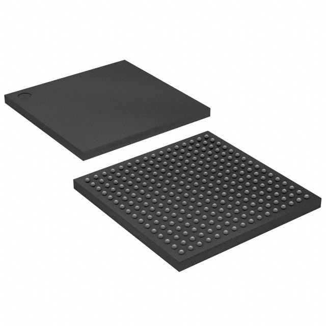
EP1C6F256C8
| Part Description |
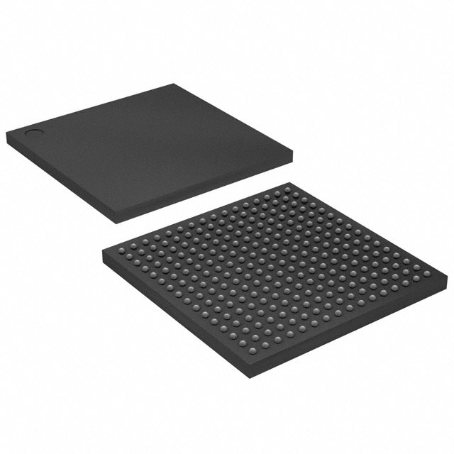
Cyclone® Field Programmable Gate Array (FPGA) IC 185 92160 5980 256-BGA |
|---|---|
| Quantity | 1,445 Available (as of October 7, 2026) |
| Product Category | Field Programmable Gate Array (FPGA) |
|---|---|
| Manufacturer | Intel |
| Manufacturing Status | Obsolete |
| Manufacturer Standard Lead Time | Contact Us |
| Datasheet |
Specifications & Environmental
| Device Package | 256-FBGA (17x17) | Grade | Commercial | Operating Temperature | 0°C – 85°C | ||
|---|---|---|---|---|---|---|---|
| Package / Case | 256-BGA | Number of I/O | 185 | Voltage | 1.425 V - 1.575 V | ||
| Mounting Method | Surface Mount | RoHS Compliance | RoHS non-compliant | REACH Compliance | REACH Unknown | ||
| Moisture Sensitivity Level | 3 (168 Hours) | Number of LABs/CLBs | 598 | Number of Logic Elements/Cells | 5980 | ||
| Number of Gates | N/A | ECCN | 3A991D | HTS Code | 8542.39.0001 | ||
| Qualification | N/A | Total RAM Bits | 92160 |
Overview of EP1C6F256C8 – Cyclone® Field Programmable Gate Array (FPGA), 185 I/O, ~92,160 bits RAM, 5,980 LEs, 256‑FBGA
The EP1C6F256C8 is a Cyclone® family SRAM-based FPGA from Intel designed for cost-sensitive data-path and logic integration applications. It provides a balance of programmable logic, embedded RAM, and I/O capacity in a compact 256‑FBGA (17×17) surface‑mount package.
Built on the Cyclone architecture, this device targets designs that require moderate logic density and on-chip memory with flexible clocking and I/O options while operating from a 1.425 V to 1.575 V supply over a commercial temperature range.
Key Features
- Logic Capacity Approximately 5,980 logic elements to implement custom logic, control, and data-path functions.
- Embedded Memory Approximately 92,160 bits of on-chip RAM (organized as 20 M4K RAM blocks) for FIFOs, buffers, and small data stores.
- I/O Density Up to 185 user I/O pins, suitable for multi‑lane interfaces, peripheral connections, and mixed-signal board-level integration.
- Clocking Two phase-locked loops (PLLs) for clock multiplication and phase shifting to support varied clock domains and timing requirements.
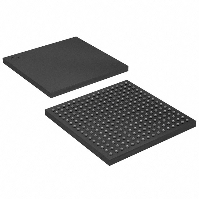
- Package 256‑FBGA (17×17) surface-mount package provides a compact footprint for space-constrained boards.
- Power Core voltage supply range: 1.425 V to 1.575 V, enabling stable device operation within the specified range.
- Operating Grade & Temperature Commercial grade with an operating temperature range of 0 °C to 85 °C.
- Standards & Family-Level Support Part of the Cyclone family which supports memory interfaces and common I/O standards (family-level capabilities include DDR interfaces, LVDS support, and PCI signaling as documented for Cyclone devices).
- Compliance RoHS compliant for lead-free assembly and environmental regulatory requirements.
Typical Applications
- Data‑Path Processing Implement custom packet processing, data formatting, or protocol bridging using the available logic elements and embedded RAM.
- Memory Interface Controllers Build DDR/SDR memory controllers and buffering logic taking advantage of on-chip RAM and the device’s clocking resources.
- Embedded Control & Glue Logic Replace multiple discrete components with programmable logic for board-level control, bus interfacing, and peripheral aggregation.
- Consumer & Industrial Electronics Use the compact 256‑FBGA package and up to 185 I/Os to integrate user interfaces, sensor aggregation, and peripheral I/O in space-constrained products.
Unique Advantages
- Balanced Logic and Memory: ~5,980 logic elements combined with ~92,160 bits of embedded RAM (20 M4K blocks) provide room for moderate complexity designs without external memory for many functions.
- Flexible I/O Count: Up to 185 user I/Os accommodate multi-signal interfaces and board-level integration while keeping a compact package footprint.
- Compact, Board-Friendly Package: The 256‑FBGA (17×17) surface-mount package enables dense board layouts for compact systems.
- Dedicated Clocking Resources: Two onboard PLLs allow designers to implement multiple clock domains and perform frequency synthesis within the device.
- Commercial-Grade Reliability: Defined commercial operating range (0 °C to 85 °C) and RoHS compliance for mainstream electronic products.
- Proven Cyclone Architecture: Leverages Cyclone family features for memory interfaces and high-speed I/O options, simplifying migration within the family.
Why Choose EP1C6F256C8?
The EP1C6F256C8 delivers a practical combination of logic density, embedded RAM, and I/O capacity in a compact 256‑FBGA package, making it well suited for designers who need programmable, board‑level integration without the overhead of higher-density devices. Its Cyclone family heritage provides familiar architecture and family-level capabilities for memory interfaces and high-speed I/O, while the included PLLs and substantial on‑chip RAM simplify clocking and buffering tasks.
This device is targeted at engineers building cost-conscious data-path, control, and interface solutions in commercial products where a balance of resources, package size, and power requirements is important.
If you would like pricing, lead-time, or availability information for EP1C6F256C8, request a quote or submit an inquiry to our team and we will respond promptly.





















Date Founded: 1968
Headquarters: Santa Clara, California, USA
Employees: 130,000+
Revenue: $54.23 Billion
Certifications and Memberships: ISO9001:2015, ISO14001:2015, ISO17025:2017, ISO27001:2022, ISO45001:2018, ISO50001:2018


