
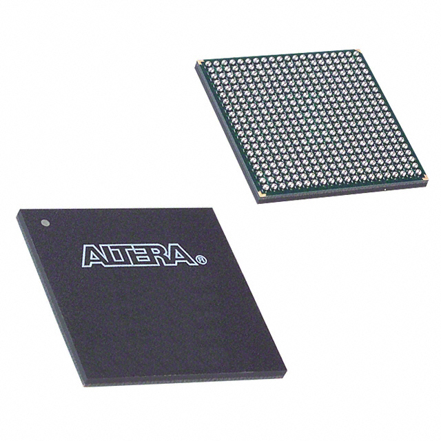
EP1C6F256C7
| Part Description |
Cyclone® Field Programmable Gate Array (FPGA) IC 185 92160 5980 256-BGA |
|---|---|
| Quantity | 577 Available (as of June 14, 2026) |

| Product Category | Field Programmable Gate Array (FPGA) |
|---|---|
| Manufacturer | Intel |
| Manufacturing Status | Obsolete |
| Manufacturer Standard Lead Time | Contact Us |
| Datasheet |
Specifications & Environmental
| Device Package | 256-FBGA (17x17) | Grade | Commercial | Operating Temperature | 0°C – 85°C | ||
|---|---|---|---|---|---|---|---|
| Package / Case | 256-BGA | Number of I/O | 185 | Voltage | 1.425 V - 1.575 V | ||
| Mounting Method | Surface Mount | RoHS Compliance | RoHS non-compliant | REACH Compliance | REACH Unknown | ||
| Moisture Sensitivity Level | 3 (168 Hours) | Number of LABs/CLBs | 598 | Number of Logic Elements/Cells | 5980 | ||
| Number of Gates | N/A | ECCN | 3A991D | HTS Code | 8542.39.0001 | ||
| Qualification | N/A | Total RAM Bits | 92160 |
Overview of EP1C6F256C7 – Cyclone® Field Programmable Gate Array (FPGA) IC 185 92160 5980 256-BGA
The EP1C6F256C7 is a Cyclone® family SRAM-based FPGA offered in a 256-BGA package designed for commercial applications. It provides a mid-range logic capacity and on-chip memory suitable for data-path and embedded-control designs that require a balance of integration and low-voltage operation.
Built on the Cyclone device architecture, this device targets applications that benefit from configurable logic, embedded RAM, multi-pin I/O and on-device clocking resources while operating within standard commercial temperature and supply ranges.
Key Features
- Logic Capacity Approximately 5,980 logic elements for implementing custom logic, glue, and control functions.
- Embedded Memory Approximately 0.092 Mbits of on-chip RAM (92,160 total bits) for local buffering and state storage.
- I/O Resources Up to 185 user I/O pins to support parallel interfaces, sensor/actuator connections, and external device control.
- Clocking Includes up to two PLLs as provided in the Cyclone family for clock multiplication and phase control.
- Package & Mounting 256-BGA (supplier package: 256-FBGA 17×17) in a surface-mount form factor for compact PCB designs.
- Power Operates from a core supply in the range 1.425 V to 1.575 V, enabling low-voltage system architectures.
- Temperature Grade Commercial operating range from 0 °C to 85 °C for standard embedded and electronics applications.
- Compliance RoHS-compliant device meeting lead-free environmental requirements.
Typical Applications
- Data-path Processing Implement custom datapath logic, packet processing, or protocol handling using the device’s logic elements and on-chip RAM.
- Memory Interfaces Support for external memory interfaces and buffering tasks that benefit from internal RAM and clocking resources.
- High-density I/O Control Drive and monitor numerous parallel signals or peripherals with the device’s 185 user I/O pins in space-constrained designs.
- Embedded Control and Glue Logic Replace multiple discrete components by consolidating control, bus bridging, and timing functions into programmable logic.
Unique Advantages
- Balanced Logic and Memory: Combines approximately 5,980 logic elements with ~92,160 bits of embedded RAM to support mixed logic and buffering requirements.
- Flexible I/O Count: 185 user I/O pins provide ample connectivity for parallel interfaces, sensor arrays, and external peripherals.
- Compact, Surface-Mount Package: 256-FBGA (17×17) delivers a space-efficient footprint for PCB designs that require high pin density.
- On-Device Clocking: Up to two PLLs enable local clock generation and phase management for synchronous designs.
- Low-Voltage Core: Core supply range of 1.425–1.575 V supports modern low-voltage system architectures.
- Commercial Availability: Commercial temperature grade and RoHS compliance make the device suitable for standard embedded and consumer electronics applications.
Why Choose EP1C6F256C7?
The EP1C6F256C7 delivers a practical combination of logic resources, embedded RAM, and extensive I/O in a compact 256-BGA package, making it a strong option for designers seeking to consolidate discrete logic and interface functions into a single configurable device. Its Cyclone family architecture provides on-device clocking and flexible I/O capability while operating within standard commercial voltage and temperature limits.
This device is well suited for development teams and OEMs building mid-range data-path, interface, or embedded control systems that require a programmable, low-voltage FPGA with a moderate logic and memory footprint and a high pin count in a surface-mount form factor.
Request a quote or submit a purchase inquiry to get pricing and availability for the EP1C6F256C7.


Date Founded: 1968
Headquarters: Santa Clara, California, USA
Employees: 130,000+
Revenue: $54.23 Billion
Certifications and Memberships: ISO9001:2015, ISO14001:2015, ISO17025:2017, ISO27001:2022, ISO45001:2018, ISO50001:2018


