
EP1C6F256C7N
| Part Description |
Cyclone® Field Programmable Gate Array (FPGA) IC 185 92160 5980 256-BGA |
|---|---|
| Quantity | 43 Available (as of June 18, 2026) |

| Product Category | Field Programmable Gate Array (FPGA) |
|---|---|
| Manufacturer | Intel |
| Manufacturing Status | Obsolete |
| Manufacturer Standard Lead Time | Contact Us |
| Datasheet |
Specifications & Environmental
| Device Package | 256-FBGA (17x17) | Grade | Commercial | Operating Temperature | 0°C – 85°C | ||
|---|---|---|---|---|---|---|---|
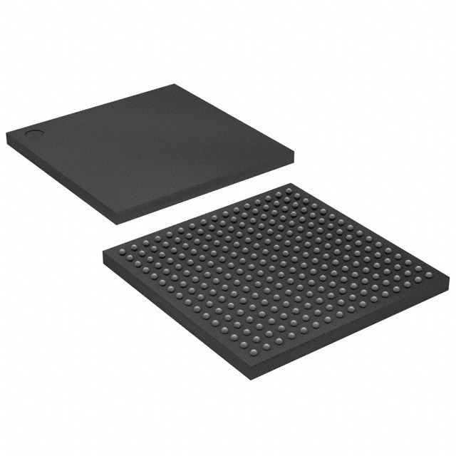
| Package / Case | 256-BGA | Number of I/O | 185 | Voltage | 1.425 V - 1.575 V | ||
| Mounting Method | Surface Mount | RoHS Compliance | Unknown | REACH Compliance | REACH Unknown | ||
| Moisture Sensitivity Level | 3 (168 Hours) | Number of LABs/CLBs | 598 | Number of Logic Elements/Cells | 5980 | ||
| Number of Gates | N/A | ECCN | 3A991D | HTS Code | 8542.39.0001 | ||
| Qualification | N/A | Total RAM Bits | 92160 |
Overview of EP1C6F256C7N – Cyclone® Field Programmable Gate Array (FPGA), 185 I/O, 5,980 logic elements, 256‑BGA
The EP1C6F256C7N is a Cyclone® series FPGA from Intel (Altera) built on a 1.5‑V, 0.13‑µm all‑layer copper SRAM process. It combines a midrange logic capacity with on‑chip RAM and configurable I/O to address data‑path, memory‑interface and system‑integration applications.
With 5,980 logic elements, approximately 92,160 bits of embedded memory and 185 user I/O pins in a space‑saving 256‑FBGA (17×17) package, this commercial‑grade device is targeted at designs that require flexible I/O standards, embedded memory and on‑chip clocking resources while operating within standard commercial temperature limits.
Key Features
- Logic Capacity — 5,980 logic elements (LEs) for implementing combinational and sequential logic in midrange FPGA designs.
- Embedded Memory — Total on‑chip RAM of 92,160 bits (approximately 0.092 Mbits) to support data buffering, FIFOs and small memory‑intensive functions.
- I/O Density and Standards — 185 user I/O pins. The Cyclone family supports multiple I/O standards including LVTTL, LVCMOS, SSTL‑2, SSTL‑3 and LVDS, enabling interfacing with a wide range of peripherals and memory devices.
- Clocking Resources — Up to two PLLs per device for clock multiplication and phase shifting, and multiple global clock resources to simplify clock distribution.
- Package and Mounting — 256‑BGA (256‑FBGA, 17×17) space‑saving package with surface mount design suitable for compact board layouts.
- Power Supply — Core voltage range specified at 1.425 V to 1.575 V for predictable power planning.
- Operating Grade — Commercial grade operation specified from 0 °C to 85 °C.
- Compliance — RoHS compliant for regulatory and environmental considerations.
Typical Applications
- Data‑path Processing — Implement midrange data‑path logic, arithmetic pipelines and protocol handlers using the device’s logic elements and embedded RAM.
- Memory Interface Controllers — Use the on‑chip memory and supported I/O standards to implement controllers for DDR SDRAM and other external memories.
- High‑speed Serial and Parallel I/O — Support LVDS and other I/O standards for high‑speed links and board‑level bridging between ASSP/ASIC devices.
- Peripheral and System Interfacing — Bridge peripherals and implement custom interfaces where flexible I/O and programmable logic are required.
Unique Advantages
- Balanced Logic and Memory — 5,980 logic elements paired with ~92 Kbits of on‑chip RAM provide a compact solution for control, buffering and small data‑storage needs.
- Flexible I/O Support — Broad I/O standard support and 185 I/O pins allow integration with a wide variety of peripherals and memory technologies.
- On‑chip Clock Management — Built‑in PLLs enable clock multiplication and phase control to meet system timing requirements without external clock conditioning.
- Compact Packaging — 256‑FBGA (17×17) package reduces PCB area and supports dense board designs while providing necessary I/O counts.
- Commercial‑grade Reliability — Specified operation from 0 °C to 85 °C for standard commercial applications and RoHS compliance for environmental alignment.
- Supported Ecosystem — Part of the Cyclone family with documented device architecture and FPGA design tool support, enabling IP reuse and design migration within the family.
Why Choose EP1C6F256C7N?
The EP1C6F256C7N positions itself as a midrange Cyclone FPGA option that combines a practical logic element count, embedded RAM and a versatile I/O complement in a compact BGA package. Its specified voltage range, PLL resources and support for common I/O standards make it suitable for designers implementing data‑path functions, memory interfaces and custom peripheral bridging in commercial applications.
For teams needing predictable commercial‑grade performance with documented family‑level tool and IP support, the EP1C6F256C7N offers a balanced platform for prototyping, integration and volume designs that require a programmable, on‑chip solution.
Request a quote or submit an inquiry to discuss availability, pricing and lead times for the EP1C6F256C7N.


Date Founded: 1968
Headquarters: Santa Clara, California, USA
Employees: 130,000+
Revenue: $54.23 Billion
Certifications and Memberships: ISO9001:2015, ISO14001:2015, ISO17025:2017, ISO27001:2022, ISO45001:2018, ISO50001:2018


