
EP1C6F256C7NAB
| Part Description |
Cyclone® Field Programmable Gate Array (FPGA) IC 185 92160 5980 256-BGA |
|---|---|
| Quantity | 1,516 Available (as of June 15, 2026) |

| Product Category | Field Programmable Gate Array (FPGA) |
|---|---|
| Manufacturer | Intel |
| Manufacturing Status | Obsolete |
| Manufacturer Standard Lead Time | Contact Us |
| Datasheet |
Specifications & Environmental
| Device Package | 256-FBGA (17x17) | Grade | Commercial | Operating Temperature | 0°C – 85°C | ||
|---|---|---|---|---|---|---|---|
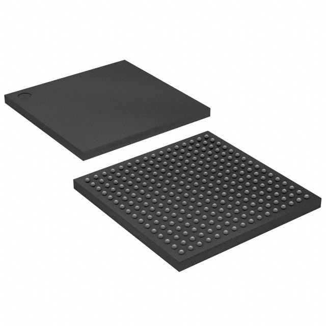
| Package / Case | 256-BGA | Number of I/O | 185 | Voltage | 1.425 V - 1.575 V | ||
| Mounting Method | Surface Mount | RoHS Compliance | Unknown | REACH Compliance | REACH Unknown | ||
| Moisture Sensitivity Level | 3 (168 Hours) | Number of LABs/CLBs | 598 | Number of Logic Elements/Cells | 5980 | ||
| Number of Gates | N/A | ECCN | OBSOLETE | HTS Code | 0000.00.0000 | ||
| Qualification | N/A | Total RAM Bits | 92160 |
Overview of EP1C6F256C7NAB – Cyclone® Field Programmable Gate Array (FPGA) IC 185 92160 5980 256-BGA
The EP1C6F256C7NAB is an Intel Cyclone® family FPGA offering a mid-range programmable logic solution optimized for data-path and system interfacing tasks. It combines 5,980 logic elements with embedded RAM and flexible I/O to address applications that require deterministic, reconfigurable hardware resources.
Built on the Cyclone architecture, this device supports integrated clock management and a variety of I/O standards, and is supplied in a compact 256-pin FineLine BGA package. Its electrical and thermal specifications support typical commercial embedded designs.
Key Features
- Core Logic 5,980 logic elements provide reconfigurable compute resources for custom data-paths, control logic, and glue logic.
- Embedded Memory Approximately 0.092 Mbits (92,160 bits) of on-chip RAM for buffering, small FIFOs, and local storage.
- I/O Capacity and Standards Up to 185 user I/O pins to interface with peripherals and external devices; device family supports LVTTL, LVCMOS, SSTL-2, SSTL-3 and LVDS I/O standards.
- Clocking and Timing Up to two integrated PLLs for clock multiplication and phase shifting to support complex timing and multi-clock designs.
- Power and Voltage Nominal core supply range 1.425 V to 1.575 V to match Cyclone family power requirements.
- Package and Mounting Surface-mount 256-pin FineLine BGA (256-FBGA, 17 × 17 mm) offering a compact footprint for space-constrained boards.
- Operating Range & Compliance Commercial-grade operating temperature 0 °C to 85 °C and RoHS-compliant manufacturing.
Typical Applications
- Data-path processing Use the programmable logic and embedded RAM for custom packet handling, protocol processing, and low-latency datapaths.
- Memory interface and buffering Implement DDR/SDR memory controllers and intermediate FIFOs leveraging on-chip RAM and available clock management.
- Peripheral bridging and interface glue Bridge between ASSPs, ASICs, and microcontrollers using the device's abundant I/O and support for common signaling standards.
- High-speed serial and parallel I/O Utilize LVDS-capable I/O and multiple pins for multi-lane links, sensor interfaces, and board-level high-speed signaling.
Unique Advantages
- Right-sized logic density: 5,980 logic elements provide a balance of capacity and cost for mid-range FPGA designs without overprovisioning.
- On-chip memory for immediate buffering: Approximately 92,160 bits of embedded RAM reduce the need for external memory in many control and buffering tasks.
- Flexible I/O and signaling: 185 user I/O pins and support for multiple standards enable straightforward integration with a wide range of peripherals and memory devices.
- Integrated clock resources: Two PLLs allow local clock generation and phase control, simplifying multi-clock and timing-critical designs.
- Compact BGA packaging: 256-FBGA (17 × 17 mm) supports high pin density in a small footprint for board-space constrained applications.
- Commercial and RoHS compliant: Commercial-grade temperature range (0 °C to 85 °C) and RoHS compliance for standard embedded product lines.
- Supported device family ecosystem: Part of the Cyclone family with documented architecture and tool support for common IP and design flows.
Why Choose EP1C6F256C7NAB?
The EP1C6F256C7NAB delivers a practical combination of reprogrammable logic, embedded memory, and flexible I/O in a compact 256-FBGA package—well suited for designers building mid-range data-paths, memory interfaces, and interface bridging solutions. Its clocking resources and I/O standard support make it adaptable to a variety of timing and signaling requirements.
This Cyclone device is positioned for customers seeking a commercially graded, RoHS-compliant FPGA with established family architecture and tool-level support, enabling scalable designs with clear migration paths across the Cyclone family.
Request a quote or submit a product inquiry to receive pricing and availability information for EP1C6F256C7NAB.


Date Founded: 1968
Headquarters: Santa Clara, California, USA
Employees: 130,000+
Revenue: $54.23 Billion
Certifications and Memberships: ISO9001:2015, ISO14001:2015, ISO17025:2017, ISO27001:2022, ISO45001:2018, ISO50001:2018


