
EP1K50FC484-3N
| Part Description |
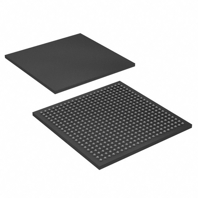
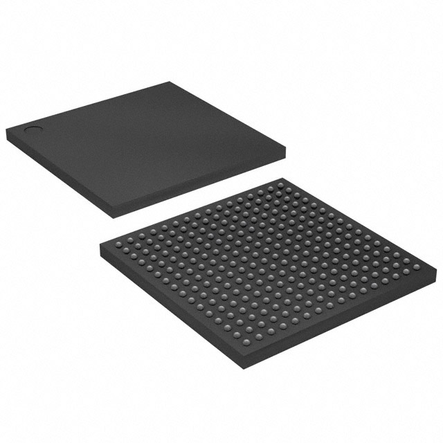
ACEX-1K® Field Programmable Gate Array (FPGA) IC 249 40960 2880 484-BBGA |
|---|---|
| Quantity | 1,593 Available (as of June 15, 2026) |

| Product Category | Field Programmable Gate Array (FPGA) |
|---|---|
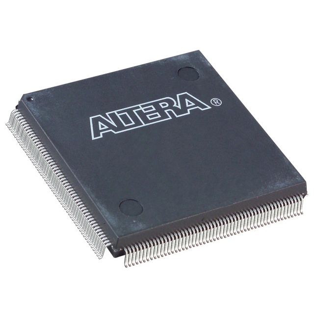
| Manufacturer | Intel |
| Manufacturing Status | Obsolete |
| Manufacturer Standard Lead Time | Contact Us |
| Datasheet |
Specifications & Environmental
| Device Package | 484-FBGA (23x23) | Grade | Commercial | Operating Temperature | 0°C – 70°C | ||
|---|---|---|---|---|---|---|---|
| Package / Case | 484-BBGA | Number of I/O | 249 | Voltage | 2.375 V - 2.625 V | ||
| Mounting Method | Surface Mount | RoHS Compliance | Unknown | REACH Compliance | REACH Unaffected | ||
| Moisture Sensitivity Level | 3 (168 Hours) | Number of LABs/CLBs | 360 | Number of Logic Elements/Cells | 2880 | ||
| Number of Gates | 199000 | ECCN | 3A991D | HTS Code | 8542.39.0001 | ||
| Qualification | N/A | Total RAM Bits | 40960 |
Overview of EP1K50FC484-3N – ACEX-1K® Field Programmable Gate Array (FPGA) IC 249 40960 2880 484-BBGA
The EP1K50FC484-3N is an Intel ACEX-1K family programmable logic device designed for system-on-a-programmable-chip (SOPC) integration. It combines a high-density logic array with embedded memory and flexible I/O to address cost-efficient communications, control and integration tasks in commercial designs.
As part of the ACEX-1K family, this device provides embedded array blocks (EABs), dual-port memory capability, and MultiVolt I/O support to simplify interfacing and on-chip megafunction implementation.
Key Features
- Logic Capacity — 2,880 logic elements delivering up to 199,000 maximum system gates for medium-density programmable logic implementations.
- Embedded Memory — Total RAM bits: 40,960 with multiple embedded array blocks (EABs) supporting dual-port operation for efficient on-chip data storage and megafunctions.
- I/O Flexibility — Up to 249 user I/O pins with MultiVolt I/O capability to drive or interface with 2.5-V, 3.3-V, or 5.0-V devices.
- Package & Mounting — 484-BBGA package (supplier package: 484-FBGA, 23×23) in a surface-mount form factor suited for compact board designs.
- Power — Operates with an internal 2.5-V supply; device voltage supply range is 2.375 V to 2.625 V.
- Temperature & Grade — Commercial grade device with an operating temperature range of 0 °C to 70 °C.
- Configuration & Test — In-circuit reconfigurability via external configuration devices, intelligent controller, or JTAG; built-in JTAG boundary-scan test (IEEE 1149.1-1990).
- Clocking & Timing — Built-in low-skew clock distribution with options such as ClockLock™ and ClockBoost™ for reduced clock delay and skew; up to six global clock signals supported.
- Routing & Arithmetic Support — FastTrack® interconnect for predictable routing delays plus dedicated carry and cascade chains for high-speed arithmetic and high-fan-in logic.
- Compliance & Environmental — RoHS compliant.
Typical Applications
- Communications Interfaces — Implement protocol bridging, bus interfaces or packet processing functions using the device’s logic capacity and flexible I/O.
- SOPC Integration — Consolidate controller, glue logic, and on-chip memory into a single device to reduce BOM and simplify system architecture.
- Embedded Memory Functions — Use dual-port EABs for fifo, buffering, or small on-chip data stores in embedded systems and peripheral controllers.
- Board-Level Prototyping and Control — Rapidly iterate control logic, interface timing, and glue logic in commercial-temperature-range designs.
Unique Advantages
- Balanced Logic and Memory — Combines 2,880 logic elements with 40,960 bits of embedded RAM to implement both control logic and on-chip data storage without external memory for many applications.
- Flexible I/O Interfacing — MultiVolt I/O support and 249 available I/O pins enable direct interfacing to a wide range of peripheral voltages and devices.
- Compact, Surface-Mount Package — 484-BBGA (23×23) packaging delivers high pin count in a compact footprint suitable for dense PCB layouts.
- Design and Test Support — JTAG boundary-scan and in-circuit reconfigurability simplify board test, field updates, and development cycles.
- Deterministic Routing and Fast Arithmetic — FastTrack® interconnect plus dedicated carry and cascade chains improve timing predictability and accelerate arithmetic implementations.
- RoHS Compliant — Meets environmental compliance requirements for lead-free assembly processes.
Why Choose EP1K50FC484-3N?
The EP1K50FC484-3N delivers a pragmatic mix of logic density, embedded memory, and flexible I/O in a compact 484-BBGA surface-mount package. Its ACEX-1K architecture is tailored for cost-efficient SOPC integration and communications-focused designs where on-chip RAM, predictable routing, and robust clocking are required.
This device is well suited for commercial designs that need medium-density programmable logic with in-circuit reconfigurability, JTAG test support, and MultiVolt interfacing. The combination of 2,880 logic elements, 40,960 bits of embedded RAM and up to 249 I/O pins offers a solid platform for consolidating peripherals and accelerating time-to-market.
Request a quote or submit an inquiry to evaluate EP1K50FC484-3N for your next design and to obtain availability and pricing information.


Date Founded: 1968
Headquarters: Santa Clara, California, USA
Employees: 130,000+
Revenue: $54.23 Billion
Certifications and Memberships: ISO9001:2015, ISO14001:2015, ISO17025:2017, ISO27001:2022, ISO45001:2018, ISO50001:2018


