
EP1K50FC484-3
| Part Description |
ACEX-1K® Field Programmable Gate Array (FPGA) IC 249 40960 2880 484-BBGA |
|---|---|
| Quantity | 411 Available (as of June 10, 2026) |

| Product Category | Field Programmable Gate Array (FPGA) |
|---|---|
| Manufacturer | Intel |
| Manufacturing Status | Obsolete |
| Manufacturer Standard Lead Time | Contact Us |
| Datasheet |
Specifications & Environmental
| Device Package | 484-FBGA (23x23) | Grade | Commercial | Operating Temperature | 0°C – 70°C | ||
|---|---|---|---|---|---|---|---|
| Package / Case | 484-BBGA | Number of I/O | 249 | Voltage | 2.375 V - 2.625 V | ||
| Mounting Method | Surface Mount | RoHS Compliance | RoHS non-compliant | REACH Compliance | REACH Unaffected | ||
| Moisture Sensitivity Level | 3 (168 Hours) | Number of LABs/CLBs | 360 | Number of Logic Elements/Cells | 2880 | ||
| Number of Gates | 199000 | ECCN | 3A991D | HTS Code | 8542.39.0001 | ||
| Qualification | N/A | Total RAM Bits | 40960 |
Overview of EP1K50FC484-3 – ACEX-1K FPGA, 2,880 logic elements, 40,960-bit embedded RAM, 249 I/O, 484‑BBGA
The EP1K50FC484-3 is an ACEX-1K® field programmable gate array (FPGA) device designed for cost-efficient system-on-a-programmable-chip (SOPC) integration. As a member of the ACEX 1K family, it combines a logic array with embedded array blocks to support megafunctions such as efficient memory and specialized logic.
This commercial-grade device targets high-volume, cost-sensitive applications where moderate logic density, on-chip RAM, and a large number of I/O pins are required. The part ships in a 484‑BBGA surface-mount package and operates over a 0 °C to 70 °C range with a supply window of 2.375 V to 2.625 V.
Key Features
- Core Logic 2,880 logic elements (LEs) and a typical gate-equivalent capacity of up to 199,000 system gates provide programmable logic for control, glue logic, and custom datapath implementations.
- Embedded Memory Approximately 40,960 bits of on-chip RAM across embedded array blocks (EABs) enable dual-port memory implementations and efficient storage for buffering and state machines.
- I/O and System-Level Support Up to 249 user I/O pins with MultiVolt I/O capability to interface with 2.5‑V, 3.3‑V, or 5.0‑V devices; features include programmable output slew-rate control, per-pin tri-state enable, and open-drain options.
- Configuration and Test In-circuit reconfigurability (ICR) via external configuration devices or the JTAG port, plus built-in JTAG boundary-scan test circuitry compliant with IEEE Std. 1149.1-1990.
- Clocking and Performance Options Low-skew clock distribution trees, options such as ClockLock™ and ClockBoost™ for reduced clock delay and skew, and dedicated carry/cascade chains for high-speed arithmetic and high-fan-in logic.
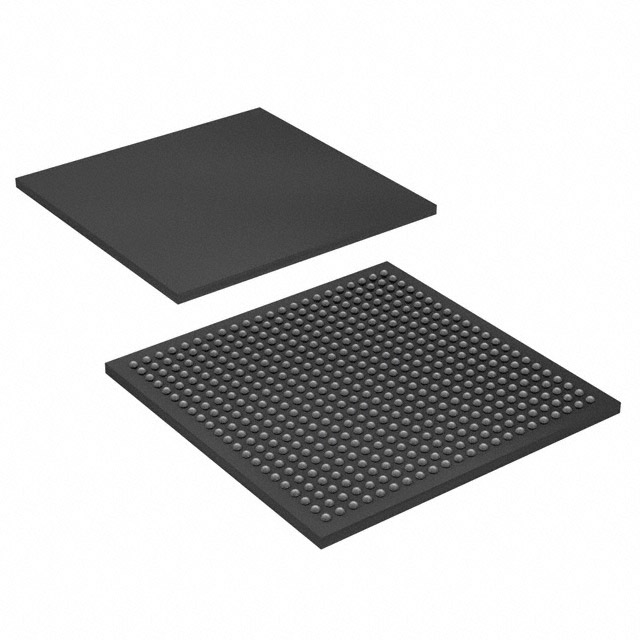
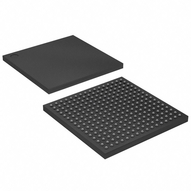
- Package & Mounting Surface-mount 484‑BBGA package (supplier device package: 484‑FBGA 23×23) for compact PCB integration in space-constrained designs.
- Power & Operating Conditions Operates with an internal 2.5‑V supply and external voltage supply range of 2.375 V to 2.625 V; commercial temperature grade specified from 0 °C to 70 °C.
- Standards & Compliance RoHS compliant and includes features for PCI Local Bus compatibility in the ACEX 1K family (3.3‑V operation) as described in the product family datasheet.
- Design Ecosystem Supported by ACEX 1K family software development tools and common EDA flows for Verilog, VHDL, and megafunction integration as documented in the family datasheet.
Typical Applications
- Communications and Networking Use for protocol bridging, buffering, and control logic in cost-sensitive communications equipment that benefit from embedded RAM and plentiful I/O.
- Embedded SOPC Integration Implement on-chip megafunctions and custom peripherals to consolidate multiple board-level functions into a single programmable device.
- PCI-Based Peripherals Suitable for 3.3‑V PCI peripherals and related interface logic where the ACEX 1K family’s PCI compliance options and I/O flexibility are useful.
- High-Volume Consumer and Commercial Devices A cost-optimized programmable logic option for designs that require moderate logic density, embedded memory, and a high pin count in a compact BGA package.
Unique Advantages
- Highly integrated solution: Combines 2,880 logic elements and approximately 40,960 bits of embedded RAM to reduce external component count and simplify system design.
- Flexible I/O interfacing: MultiVolt I/O and per-pin features (tri-state enable, open-drain, programmable slew) enable direct interfacing to a variety of external device voltages.
- Robust configuration and test: JTAG boundary-scan and in-circuit reconfigurability support production testing and field reprogramming without consuming device logic.
- Clock and arithmetic optimizations: Dedicated carry and cascade chains plus low-skew clock trees help implement fast adders, counters, and high-fan-in logic efficiently.
- Compact, manufacturable package: 484‑BBGA surface-mount package provides a high I/O count in a compact footprint suitable for automated high-volume assembly.
- RoHS compliant: Meets RoHS requirements for lead-free manufacturing and regulatory compliance in commercial products.
Why Choose EP1K50FC484-3?
The EP1K50FC484-3 delivers a balanced combination of programmable logic capacity, embedded memory, and a large I/O complement in a compact 484‑BBGA package. It is positioned for designers who need a cost-efficient FPGA solution for SOPC integration, communications interfaces, and PCI-related peripherals within commercial-temperature applications.
Backed by ACEX 1K family design support and tools, this device offers predictable routing, dedicated arithmetic resources, and configuration options that help shorten development time and reduce BOM complexity for medium-density programmable designs.
Request a quote or submit an RFQ for EP1K50FC484-3 to evaluate fit for your next design and obtain pricing and availability information.


Date Founded: 1968
Headquarters: Santa Clara, California, USA
Employees: 130,000+
Revenue: $54.23 Billion
Certifications and Memberships: ISO9001:2015, ISO14001:2015, ISO17025:2017, ISO27001:2022, ISO45001:2018, ISO50001:2018


