
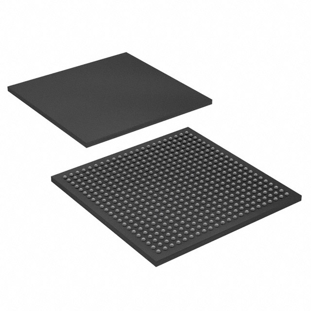
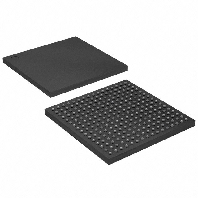
EP1K50FC484-2
| Part Description |
ACEX-1K® Field Programmable Gate Array (FPGA) IC 249 40960 2880 484-BBGA |
|---|---|
| Quantity | 198 Available (as of June 17, 2026) |

| Product Category | Field Programmable Gate Array (FPGA) |
|---|---|
| Manufacturer | Intel |
| Manufacturing Status | Obsolete |
| Manufacturer Standard Lead Time | Contact Us |
| Datasheet |
Specifications & Environmental
| Device Package | 484-FBGA (23x23) | Grade | Commercial | Operating Temperature | 0°C – 70°C | ||
|---|---|---|---|---|---|---|---|
| Package / Case | 484-BBGA | Number of I/O | 249 | Voltage | 2.375 V - 2.625 V | ||
| Mounting Method | Surface Mount | RoHS Compliance | RoHS non-compliant | REACH Compliance | REACH Unaffected | ||
| Moisture Sensitivity Level | 3 (168 Hours) | Number of LABs/CLBs | 360 | Number of Logic Elements/Cells | 2880 | ||
| Number of Gates | 199000 | ECCN | 3A991D | HTS Code | 8542.39.0001 | ||
| Qualification | N/A | Total RAM Bits | 40960 |
Overview of EP1K50FC484-2 – ACEX-1K® Field Programmable Gate Array (FPGA) IC 249 40960 2880 484-BBGA
The EP1K50FC484-2 is an ACEX-1K family field programmable gate array (FPGA) from Intel, designed for cost-efficient system-on-a-programmable-chip (SOPC) integration. It combines a dedicated logic array and embedded memory resources to implement megafunctions, dual-port memory, and general-purpose logic in a single surface-mount device.
With 2,880 logic elements, approximately 40,960 bits of embedded RAM, and up to 249 I/O pins in a 484-BBGA package, this device targets high-density, high-integration applications that require flexible I/O, in-circuit reconfigurability, and a compact BOM footprint.
Key Features
- Logic Capacity — 2,880 logic elements and a maximum of approximately 199,000 system gates provide substantial on-chip logic for control, state machines, and custom datapaths.
- Embedded Memory — Approximately 40,960 bits of RAM and multiple embedded array blocks (EABs) support dual-port memory configurations and efficient implementation of on-chip buffers and FIFOs.
- I/O and Voltage — Up to 249 user I/O pins with MultiVolt I/O capability; device operates with an internal 2.5-V supply and a specified supply range of 2.375 V to 2.625 V.
- Package and Mounting — Surface-mount 484-BBGA (supplier package 484-FBGA, 23×23) for high-density board layouts and reliable fine-pitch mounting.
- Clocking and Performance — Built-in low-skew clock distribution trees and options for reduced clock delay and skew support synchronous designs and higher-frequency I/O timing.
- Configuration and Test — In-circuit reconfigurability via external configuration devices or JTAG; built-in JTAG boundary-scan test (IEEE 1149.1) for board-level testability without consuming user logic.
- Compliance and Environmental — Commercial grade operation from 0 °C to 70 °C; RoHS compliant material and manufacturing.
Typical Applications
- Communications Equipment — Implement protocol bridging, packet buffering, and interface logic using embedded RAM and abundant I/O to reduce external components.
- SOPC and Megafunction Integration — Integrate memory-intensive megafunctions and custom logic in a single device for compact system designs.
- PCI and Bus Interface Logic — Use the device in bus interface and local bus applications leveraging the family’s PCI compatibility features at supported voltage levels.
- In-System Programmable Designs — Take advantage of in-circuit reconfigurability and JTAG for field updates, iterative development, and board-level testing.
Unique Advantages
- Highly integrated solution: 2,880 logic elements and approximately 40,960 bits of embedded RAM reduce the need for external glue logic and discrete memory, simplifying PCB design.
- Flexible I/O and Voltage support: Up to 249 I/O pins plus MultiVolt I/O capability enable direct interfacing to a wide range of voltage domains and legacy peripherals.
- Compact, board-friendly package: 484-BBGA surface-mount package provides high pin density in a compact footprint for space-constrained designs.
- Design and testability: Integrated JTAG boundary-scan and in-circuit reconfigurability streamline manufacturing test and field updates without consuming user logic.
- Vendor ecosystem and tools support: ACEX-1K family design support includes synthesis, place-and-route, and megafunction libraries to accelerate development and migration within the family.
- Regulatory and environmental compliance: RoHS compliant manufacturing and commercial temperature grading align with common electronics industry requirements.
Why Choose EP1K50FC484-2?
The EP1K50FC484-2 positions itself as a practical, high-density FPGA choice for designers seeking to consolidate memory and logic into a single programmable device. Its balance of logic elements, embedded RAM, and abundant I/O in a compact 484-BBGA package makes it well suited for communications, bus-interface, and SOPC-style implementations where board space and BOM count are critical.
Backed by Intel’s ACEX-1K family development ecosystem and proven configuration and test features, the EP1K50FC484-2 offers a scalable platform for mid-range FPGA designs that require field reconfiguration, reliable board testability, and commercial-grade operation.
Request a quote or submit a purchase inquiry for the EP1K50FC484-2 to receive pricing and availability details for your project.


Date Founded: 1968
Headquarters: Santa Clara, California, USA
Employees: 130,000+
Revenue: $54.23 Billion
Certifications and Memberships: ISO9001:2015, ISO14001:2015, ISO17025:2017, ISO27001:2022, ISO45001:2018, ISO50001:2018


