
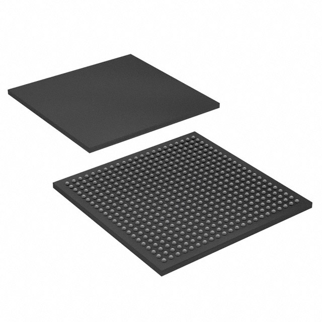
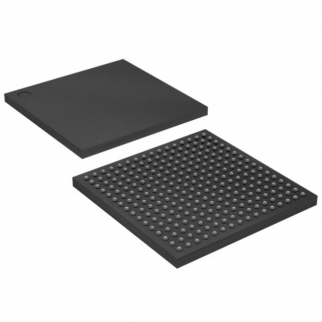
EP1K50FC484-1
| Part Description |
ACEX-1K® Field Programmable Gate Array (FPGA) IC 249 40960 2880 484-BBGA |
|---|---|
| Quantity | 107 Available (as of June 15, 2026) |

| Product Category | Field Programmable Gate Array (FPGA) |
|---|---|
| Manufacturer | Intel |
| Manufacturing Status | Obsolete |
| Manufacturer Standard Lead Time | Contact Us |
| Datasheet |
Specifications & Environmental
| Device Package | 484-FBGA (23x23) | Grade | Commercial | Operating Temperature | 0°C – 70°C | ||
|---|---|---|---|---|---|---|---|
| Package / Case | 484-BBGA | Number of I/O | 249 | Voltage | 2.375 V - 2.625 V | ||
| Mounting Method | Surface Mount | RoHS Compliance | RoHS non-compliant | REACH Compliance | REACH Unaffected | ||
| Moisture Sensitivity Level | 3 (168 Hours) | Number of LABs/CLBs | 360 | Number of Logic Elements/Cells | 2880 | ||
| Number of Gates | 199000 | ECCN | 3A991D | HTS Code | 8542.39.0001 | ||
| Qualification | N/A | Total RAM Bits | 40960 |
Overview of EP1K50FC484-1 – ACEX-1K® Field Programmable Gate Array (FPGA) IC, 249 I/O, 40,960-bit RAM, 2,880 Logic Elements, 484-BBGA
The EP1K50FC484-1 is an Intel ACEX-1K family field programmable gate array (FPGA) designed for cost-efficient system-on-a-programmable-chip (SOPC) integration. It combines a dense logic array with embedded memory blocks to implement control logic, interfaces, and megafunctions in a single, reconfigurable device.
Targeted at commercial applications requiring medium-density programmable logic, this device delivers 2,880 logic elements, approximately 40,960 bits of embedded RAM, and up to 249 user I/O pins in a compact 484-ball BGA package. It supports a 2.5 V internal supply and a 2.375 V–2.625 V external supply range, with operation specified for 0 °C to 70 °C.
Key Features
- Programmable Logic Capacity 2,880 logic elements and an internal architecture suited for implementing general logic functions and megafunctions.
- Embedded Memory (EABs) Approximately 40,960 bits of total RAM provided by embedded array blocks, including dual-port capability for flexible memory interfacing.
- I/O Flexibility Up to 249 user I/O pins to support a wide range of peripheral and bus interfacing requirements.
- Performance and Timing Options Built-in low-skew clock distribution, ClockLock and ClockBoost options to manage clock delay and skew for timing-critical designs.
- System Integration Supports in-circuit reconfigurability via external configuration devices, an intelligent controller, or the JTAG port (IEEE 1149.1-1990 compliant), enabling field updates and development flexibility.
- Power and Voltage Operates with a 2.5 V internal supply and an external supply range of 2.375 V to 2.625 V for core power.
- Package and Mounting Available in a 484-BBGA package (supplier package: 484-FBGA, 23×23); surface-mount mounting type for compact board designs.
- Compliance and Reliability RoHS compliant and 100% functionally tested at the device level; includes JTAG boundary-scan test circuitry without consuming device logic.
- Commercial Temperature Grade Specified for operation from 0 °C to 70 °C for commercial applications.
Typical Applications
- Communications Interfaces Implement protocol bridging, peripheral interfaces, or custom data-path logic leveraging the device’s embedded RAM and flexible I/O complement.
- System-on-a-Programmable-Chip (SOPC) Integrate control logic, memory buffers, and specialized megafunctions to reduce board-level component count in cost-sensitive designs.
- High-Volume Consumer and Commercial Products Use the device where a medium-density, reconfigurable logic solution lowers BOM and supports in-field updates through in-circuit reconfiguration.
- Timing-Critical Control Logic Take advantage of low-skew clock trees, dedicated carry/cascade chains, and clock management options for deterministic timing in control and signal-processing paths.
Unique Advantages
- Balanced Logic and Memory: 2,880 logic elements paired with approximately 40,960 bits of embedded RAM provide a balanced platform for mixed logic-and-memory designs without external SRAM for many applications.
- Flexible I/O Count: Up to 249 user I/O pins allow integration of multiple peripherals and buses on a single device, simplifying board-level routing and connectors.
- Reconfigurability in-Circuit: Support for in-circuit reconfiguration and JTAG programming enables iterative development and field updates without replacing hardware.
- Clocking Options for Determinism: Built-in low-skew distribution plus ClockLock/ClockBoost options help reduce clock delay and skew, aiding reliable timing closure.
- Compact BGA Packaging: The 484-BBGA package offers a high pin count in a compact footprint, helping reduce PCB area in space-constrained designs.
- Proven Device-Level Testing: 100% functional testing at the device level and built-in JTAG boundary-scan support enhance board-level testability and yield.
Why Choose EP1K50FC484-1?
The EP1K50FC484-1 positions itself as a medium-density, commercially graded FPGA solution for designs that require a combination of programmable logic, embedded memory, and a substantial I/O complement in a compact BGA package. Its feature set—including in-circuit reconfigurability, dual-port embedded arrays, dedicated carry and cascade chains, and clock management options—helps shorten development cycles and consolidate functions that would otherwise require multiple components.
This device is well suited to engineers developing cost-sensitive, high-volume commercial products where the balance of logic resources, on-chip RAM, and flexible I/O can simplify system architecture and reduce bill-of-materials and board complexity while retaining the ability to update functionality in the field.
Request a quote or submit an inquiry to get pricing, availability, and ordering information for EP1K50FC484-1.


Date Founded: 1968
Headquarters: Santa Clara, California, USA
Employees: 130,000+
Revenue: $54.23 Billion
Certifications and Memberships: ISO9001:2015, ISO14001:2015, ISO17025:2017, ISO27001:2022, ISO45001:2018, ISO50001:2018


